
Datasheet

HEF4794B All information provided in this document is subject to legal disclaimers. © NXP B.V. 2011. All rights reserved.
Product data sheet Rev. 7 — 16 November 2011 4 of 18
NXP Semiconductors
HEF4794B
8-stage shift-and-store register LED driver
6. Functional description
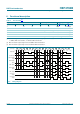
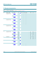
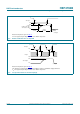
[1] H = HIGH voltage level; L = LOW voltage level; X = don’t care; Z = high-impedance OFF-state;
= LOW-to-HIGH clock transition; = HIGH-to-LOW clock transition.
[2] Q6S = the data in register stage 6 before the LOW to HIGH clock transition.
[3] Q7S = the data in register stage 7 before the HIGH to LOW clock transition.
Table 3. Function table
[1]
Input Parallel output Serial output
CP OE STR D QP0 QPn QS1
[2]
QS2
[3]
L X X Z Z Q6S no change
LXXZZn.c.Q7S
H L X no change no change Q6S no change
HHL ZQPn 1 Q6S no change
HHHL QPn 1 Q6S no change
H H H no change no change no change Q7S
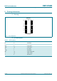
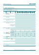
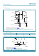
Fig 5. Timing diagram
001aag801
clock input
data input
strobe input
output enable
input
internal Q0S
(FF0)
QP0 output
internal Q6S
(FF6)
QP6 output
serial QS1
output
serial QS2
output
Z-state
Z-state