
Datasheet

HEF4794B All information provided in this document is subject to legal disclaimers. © NXP B.V. 2011. All rights reserved.
Product data sheet Rev. 7 — 16 November 2011 8 of 18
NXP Semiconductors
HEF4794B
8-stage shift-and-store register LED driver
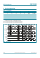
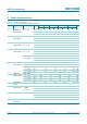
[1] The typical values of the propagation delay and transition times are calculated from the extrapolation formulas shown (C
L
in pF).
[2] t
en
is the same as t
PZL
and t
dis
is the same as t
PLZ
[3] t
t
is the same as t
TLH
and t
THL
t
W
pulse width CP; LOW and
HIGH;
see Figure 6
5 V 60 30 - ns
10 V 30 15 - ns
15 V 24 12 - ns
STR; HIGH;
see Figure 7
5 V 80 40 - ns
10 V 60 30 - ns
15 V 24 12 - ns
t
su
set-up time D to CP;
see Figure 9
5 V 60 30 - ns
10 V 20 10 - ns
15 V 15 5 - ns
t
h
hold time D to CP;
see Figure 9
5 V +5 15 - ns
10 V 20 5 - ns
15 V 20 5 - ns
f
clk(max)
maximum clock
frequency
CP; see Figure 6 5 V 5 10 - MHz
10 V 11 22 - MHz
15 V 14 28 - MHz
Table 7. Dynamic characteristics
…continued
V
SS
= 0 V; T
amb
= 25
C unless otherwise specified. For test circuit, see Figure 10.
Symbol Parameter Conditions V
DD
Extrapolation formula Min Typ Max Unit
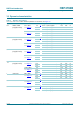
Table 8. Dynamic power dissipation
P
D
can be calculated from the formulas shown. V
SS
= 0 V; t
r
= t
f
20 ns; T
amb
= 25
C.
Symbol Parameter V
DD
Typical formula Where
P
D
dynamic power dissipation 5 V P
D
= 1200 f
i
+ (f
o
C
L
) V
DD
2
Wf
i
= input frequency in MHz;
f
o
= output frequency in MHz;
C
L
= output load capacitance in pF;
(f
o
C
L
) = sum of the outputs;
V
DD
= supply voltage in V.
10 V P
D
= 5550 f
i
+ (f
o
C
L
) V
DD
2
W
15 V P
D
= 15000 f
i
+ (f
o
C
L
) V
DD
2
W