
Datasheet

HEF4794B All information provided in this document is subject to legal disclaimers. © NXP B.V. 2011. All rights reserved.
Product data sheet Rev. 7 — 16 November 2011 9 of 18
NXP Semiconductors
HEF4794B
8-stage shift-and-store register LED driver
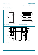
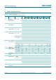
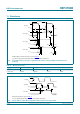
11. Waveforms
Parallel output measurement points are given in Table 9.
V
OL
and V
OH
are typical output voltage levels that occur with the output load.
Fig 6. Propagation delay clock (CP) to output (QPn, QS1, QS2), clock pulse width and maximum clock
frequency
001aag222
t
PLH
1/f
clk(max)
V
M
V
M
V
X
V
I
V
SS
V
DD
V
OL
V
OL
V
OL
t
W
t
PLZ
t
PLH
t
PZL
V
Y
CP input
QS1 output
QS2 output
t
THL
t
TLH
90 %
10 %
V
M
90 %
10 %
t
PHL
t
THL
t
TLH
QPn output
t
W
t
PHL
V
OH
V
OH
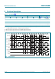
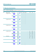
Table 9. Measurement points
Supply Input Output
V
DD
V
M
V
M
V
X
V
Y
5 V to 15 V 0.5V
DD
0.5V
DD
0.1V
O
0.9V
O
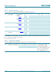
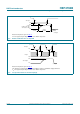
Measurement points are given in Table 9.
V
OL
is the typical output voltage level that occurs with the output load.
Fig 7. Strobe (STR) to output (QPn) propagation delays and the strobe pulse width
001aag802
CP input
t
W
t
PLZ
t
PZL
V
M
V
M
V
X
V
Y
V
I
V
SS
V
I
V
SS
STR input
V
DD
V
OL
QPn output