
User's Manual
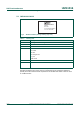
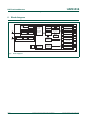

Table Of Contents
- 1. General description
- 2. Features and benefits
- 3. Applications
- 4. Overview
- 5. Marking
- 6. Block diagram
- 7. Pinning information
- 8. Functional description
- 9. Limiting values
- 10. Recommended operating conditions
- 11. Characteristics
- 12. Federal Communication Commission Statement
- 13. Industry Canada statement
- 14. Footprint information for reflow soldering
- 15. Package outline
- 16. Abbreviations
- 17. References
- 18. Legal information
- 19. Tables
- 20. Figures
- 21. Contents

UM11016 All information provided in this document is subject to legal disclaimers. © NXP Semiconductors N.V. 2016. All rights reserved.
User manual Rev. 1.0 — 15 June 2016 4 of 24
NXP Semiconductors
UM11016
ZigBee PRO and IEEE802.15.4 JN5169-001-M0x-2 modules
• Ready to use in products
• Minimises product development time
• No RF test required for systems
• Compliant with:
– FCC 47CFR Part 15C
– ETSI EN 300-328 V1.9.1
– EN 301-489-17 V2.2.1
– EN60950-1-2006
– ANATEL
• Temperature range: 40 C to +85 C
• Lead-free and RoHS compliant
2.2 Features: modules
• 2.4 GHz IEEE 802.15.4, ZigBee Smart Energy and Home Automation compatible
• JN5169-001-M00-2
– Dimensions: 16 mm 30 mm
– Integrated printed antenna
– TX power 8.5 dBm/10 dBm
– Receiver sensitivity –96.5 dBm
– TX current 27.2 mA at 10 dBm
– TX current 23.6 mA at 8.5 dBm
– RX current 17.8 mA at maximum input level 10 dBm
– RX current 16.2 mA at maximum input level 0 dBm
– 2.0 V/3.6 V operation
• JN5169-001-M03-2
– Dimensions: 16 mm 21 mm
– Fl connector
– TX power 8.5 dBm/10 dBm
– Receiver sensitivity –96.5 dBm
– TX current 27.2 mA at 10 dBm
– TX current 23.6 mA at 8.5 dBm
– RX current 17.8 mA at maximum input level 10 dBm
– RX current 16.2 mA at maximum input level 0 dBm
– 2.0 V/3.6 V operation
• JN5169-001-M06-2
– Dimensions: 16 mm 30 mm
– Fl connector
– TX power 21 dBm
– Receiver sensitivity –100 dBm