
Datasheet

KMZ60 All information provided in this document is subject to legal disclaimers. © NXP B.V. 2014. All rights reserved.
Product data sheet Rev. 2 — 7 February 2014 10 of 30
NXP Semiconductors
KMZ60
Angle sensor with integrated amplifier
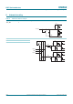
[1] Between pin V
CC
and pin GND, soldered close to the package.
[2] Operating as sink or source.
[3] Between pin VOUT1 and pin V
CC
or pin GND and between pin VOUT2 and pin V
CC
or pin GND.
[4] Short-circuit to pin GND within a time limit of 10 minutes.
[5] Short-circuit to pin V
CC
within a time limit of 10 minutes.
[6] Induced voltage from a rotating strong magnetic field may impact the performance but without damage.
[7] Angle error due to reference position defined by the leadframe, sample based controlled at assembly line.
[8] By calculation of peak-to-peak amplitude relation k = 100 V
o(VOUT1)
/V
o(VOUT2)
.
[9] Rotation frequency dependent phase error, after offset correction, amplitude calibration and arctangent calculation.
[10] Value calculated only with third and fifth harmonic of the spectrum of output signal amplitude V
o(VOUT1)
and V
o(VOUT2)
by ideal
homogeneous field.
[11] Maximum limit is valid with external first order filter of 80 kHz.
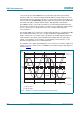
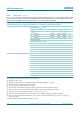
Temperature dependency of signal outputs without TC compensation (pin TCC_EN to ground)
V
o
output voltage peak-to-peak value;
on pin VOUT1; R
L(o)ext
=5k
T
amb
= 40 C 0.54V
CC
0.66V
CC
0.76V
CC
V
T
amb
=25C 0.41V
CC
0.49V
CC
0.57V
CC
V
T
amb
=85C 0.31V
CC
0.37V
CC
0.45V
CC
V
T
amb
=105C 0.275V
CC
0.34V
CC
0.425V
CC
V
T
amb
=150C 0.21V
CC
0.27V
CC
0.36V
CC
V
peak-to-peak value;
on pin VOUT2; R
L(o)ext
=5k
T
amb
= 40 C 0.54V
CC
0.66V
CC
0.76V
CC
V
T
amb
=25C 0.41V
CC
0.49V
CC
0.57V
CC
V
T
amb
=85C 0.31V
CC
0.37V
CC
0.45V
CC
V
T
amb
=105C 0.275V
CC
0.34V
CC
0.425V
CC
V
T
amb
=150C 0.21V
CC
0.27V
CC
0.36V
CC
V
V
offset
offset voltage on pin VOUT1; R
L(o)ext
=5k
T
amb
= 40 C 0.07V
CC
-+0.07V
CC
V
T
amb
=25C 0.07V
CC
-+0.07V
CC
V
T
amb
=85C 0.07V
CC
-+0.07V
CC
V
T
amb
=105C 0.075V
CC
- +0.075V
CC
V
T
amb
=150C 0.08V
CC
-+0.08V
CC
V
on pin VOUT2; R
L(o)ext
=5k
T
amb
= 40 C 0.07V
CC
-+0.07V
CC
V
T
amb
=25C 0.07V
CC
-+0.07V
CC
V
T
amb
=85C 0.07V
CC
-+0.07V
CC
V
T
amb
=105C 0.075V
CC
- +0.075V
CC
V
T
amb
=150C 0.08V
CC
-+0.08V
CC
V
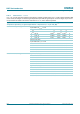
Table 7. Characteristics
…continued
T
amb
=25
C; angle accuracies referred to homogeneous excitation magnetic fields of H
ext
= 25 kA/m directed parallel to MR
sensor surface; all voltages are related to ground potential of pin GND; the signal outputs and offset voltages on pin VOUT1
and pin VOUT2 are related to the common mode level of V
CC
/ 2; unless otherwise specified.
Symbol Parameter Conditions Min Typ Max Unit