
Datasheet


LM75A_4 © NXP B.V. 2007. All rights reserved.
Product data sheet Rev. 04 — 10 July 2007 5 of 24
NXP Semiconductors
LM75A
Digital temperature sensor and thermal watchdog
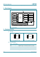
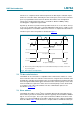
In both cases, comparator mode and interrupt mode, the OS output is activated only if a
number of consecutive faults, defined by the device fault queue, has been met. The fault
queue is programmable and stored in the two bits, B3 and B4, of the Configuration
register. Also, the OS output active state is selectable as HIGH or LOW by setting
accordingly the configuration register bit B2.
At power-up, the device is put into normal operation mode, the T
os
is set to 80 °C, the T
hyst
is set to 75 °C, the OS active state is selected LOW and the fault queue is equal to 1. The
temp reading data is not available until the first conversion is completed in about 100 ms.
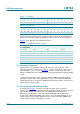
The OS response to the temperature is illustrated in Figure 4.
7.2 I
2
C-bus serial interface
The LM75A can be connected to a compatible 2-wire serial interface I
2
C-bus as a slave
device under the control of a controller or master device, using two device terminals, SCL
and SDA. The controller must provide the SCL clock signal and write/read data to/from the
device through the SDA terminal. Notice that if the I
2
C-bus common pull-up resistors have
not been installed as required for I
2
C-bus, then an external pull-up resistor, about 10 kΩ,
is needed for each of these two terminals. The bus communication protocols are
described in Section 7.10.
7.3 Slave address
The LM75A slave address on the I
2
C-bus is partially defined by the logic applied to the
device address pins A2, A1 and A0. Each of them is typically connected either to GND for
logic 0, or to V
CC
for logic 1. These pins represent the three LSB bits of the device 7-bit
address. The other four MSB bits of the address data are preset to ‘1001’ by hard wiring
inside the LM75A. Table 4 shows the device’s complete address and indicates that up to
(1) OS is reset by either reading register. It is assumed that the fault queue is met at each T
os
and
T
hyst
crossing point.
Fig 4. OS response to temperature
002aad032
(1) (1) (1)
T
os
T
hyst
OS reset
OS active
OS reset
OS active
OS output in comparator mode
OS output in interrupt mode
reading temperature limits