
Datasheet

LM75B All information provided in this document is subject to legal disclaimers. © NXP B.V. 2015. All rights reserved.
Product data sheet Rev. 6.1 — 6 February 2015 5 of 37
NXP Semiconductors
LM75B
Digital temperature sensor and thermal watchdog
6.2 Pin description
7. Functional description
7.1 General operation
The LM75B uses the on-chip band gap sensor to measure the device temperature with
the resolution of 0.125 C and stores the 11-bit two’s complement digital data, resulted
from 11-bit A-to-D conversion, into the device Temp register. This Temp register can be
read at any time by a controller on the I
2
C-bus. Reading temperature data does not affect
the conversion in progress during the read operation.
The device can be set to operate in either mode: normal or shutdown. In normal operation
mode, the temp-to-digital conversion is executed every 100 ms and the Temp register is
updated at the end of each conversion. During each ‘conversion period’ (T
conv
) of about
100 ms the device takes only about 10 ms, called ‘temperature conversion time’ (t
conv(T)
),
to complete a temperature-to-data conversion and then becomes idle for the time
remaining in the period. This feature is implemented to significantly reduce the device
power dissipation. In shutdown mode, the device becomes idle, data conversion is
disabled and the Temp register holds the latest result; however, the device I
2
C-bus
interface is still active and register write/read operation can be performed. The device
operation mode is controllable by programming bit B0 of the configuration register. The
temperature conversion is initiated when the device is powered-up or put back into normal
mode from shutdown.
In addition, at the end of each conversion in normal mode, the temperature data (or Temp)
in the Temp register is automatically compared with the overtemperature shutdown
threshold data (or T
th(ots)
) stored in the Tos register, and the hysteresis data (or T
hys
)
stored in the Thyst register, in order to set the state of the device OS output accordingly.
The device Tos and Thyst registers are write/read capable, and both operate with 9-bit
two’s complement digital data. To match with this 9-bit operation, the Temp register uses
only the 9 MSB bits of its 11-bit data for the comparison.
The way that the OS output responds to the comparison operation depends upon the OS
operation mode selected by configuration bit B1, and the user-defined fault queue defined
by configuration bits B3 and B4.
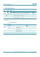
Table 3. Pin description
Symbol Pin Description
SDA 1 Digital I/O. I
2
C-bus serial bidirectional data line; open-drain.
SCL 2 Digital input. I
2
C-bus serial clock input.
OS 3 Overtemperature Shutdown output; open-drain.
GND 4 Ground. To be connected to the system ground.
A2 5 Digital input. User-defined address bit 2.
A1 6 Digital input. User-defined address bit 1.
A0 7 Digital input. User-defined address bit 0.
V
CC
8 Power supply.