
Datasheet

LM75B All information provided in this document is subject to legal disclaimers. © NXP B.V. 2015. All rights reserved.
Product data sheet Rev. 6.1 — 6 February 2015 7 of 37
NXP Semiconductors
LM75B
Digital temperature sensor and thermal watchdog
7.2 I
2
C-bus serial interface
The LM75B can be connected to a compatible 2-wire serial interface I
2
C-bus as a slave
device under the control of a controller or master device, using two device terminals, SCL
and SDA. The controller must provide the SCL clock signal and write/read data to/from the
device through the SDA terminal. Notice that if the I
2
C-bus common pull-up resistors have
not been installed as required for I
2
C-bus, then an external pull-up resistor, about 10 k,
is needed for each of these two terminals. The bus communication protocols are
described in Section 7.10
.
7.2.1 Bus fault time-out
If the SDA line is held LOW for longer than t
to
(75 ms minimum / 13.3 Hz; guaranteed at
50 ms minimum / 20 Hz), the LM75B will reset to the idle state (SDA released) and wait
for a new START condition. This ensures that the LM75B will never hang up the bus
should there be conflict in the transmission sequence.
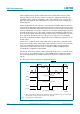
7.3 Slave address
The LM75B slave address on the I
2
C-bus is partially defined by the logic applied to the
device address pins A2, A1 and A0. Each of them is typically connected either to GND for
logic 0, or to V
CC
for logic 1. These pins represent the three LSB bits of the device 7-bit
address. The other four MSB bits of the address data are preset to ‘1001’ by hard wiring
inside the LM75B. Table 4
shows the device’s complete address and indicates that up to
8 devices can be connected to the same bus without address conflict. Because the input
pins, SCL, SDA and A2 to A0, are not internally biased, it is important that they should not
be left floating in any application.
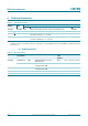
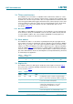
7.4 Register list
The LM75B contains four data registers beside the pointer register as listed in Table 5.
The pointer value, read/write capability and default content at power-up of the registers
are also shown in Table 5
.
Table 4. Address table
1 = HIGH; 0 = LOW.
MSB LSB
1 0 0 1 A2 A1 A0
Table 5. Register table
Register
name
Pointer
value
R/W POR
state
Description
Conf 01h R/W 00h Configuration register: contains a single 8-bit data
byte; to set the device operating condition; default = 0.
Temp 00h read only n/a Temperature register: contains two 8-bit data bytes;
to store the measured Temp data.
Tos 03h R/W 5000h Overtemperature shutdown threshold register:
contains two 8-bit data bytes; to store the
overtemperature shutdown T
th(ots)
limit;
default = 80 C.
Thyst 02h R/W 4B00h Hysteresis register: contains two 8-bit data bytes;
to store the hysteresis T
hys
limit; default = 75 C.