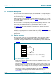
PCF2127AT Integrated RTC, TCXO and quartz crystal Rev. 6 — 11 July 2013 Product data sheet 1. General description The PCF2127AT1 is a CMOS2 Real Time Clock (RTC) and calendar with an integrated Temperature Compensated Crystal (Xtal) Oscillator (TCXO) and a 32.768 kHz quartz crystal optimized for very high accuracy and very low power consumption.
PCF2127AT NXP Semiconductors Integrated RTC, TCXO and quartz crystal Clock operating voltage: 1.2 V to 4.2 V Low supply current: typical 0.65 A at VDD = 3.0 V and Tamb = 25 C 3. Applications Electronic metering for electricity, water, and gas Precision timekeeping Access to accurate time of the day GPS equipment to reduce time to first fix Applications that require an accurate process timing Products with long automated unattended operation time 4. Ordering information Table 1.
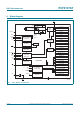
PCF2127AT NXP Semiconductors Integrated RTC, TCXO and quartz crystal 6.
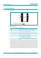
PCF2127AT NXP Semiconductors Integrated RTC, TCXO and quartz crystal 7. Pinning information 7.1 Pinning SCL 1 SDI 2 20 VDD 19 VBAT SDO 3 18 BBS SDA/CE 4 17 INT IFS 5 TS 6 CLKOUT 7 14 PFO VSS 8 13 TEST n.c. 9 12 n.c. n.c. 10 11 n.c. PCF2127AT 16 RST 15 PFI 001aaj676 Top view. For mechanical details, see Figure 53. Fig 2. Pin configuration for SO20 (PCF2127AT) 7.2 Pin description Table 4.
PCF2127AT NXP Semiconductors Integrated RTC, TCXO and quartz crystal Table 4. Pin description of SO20 (PCF2127AT) …continued Symbol Pin Description BBS 18 output voltage (battery backed) VBAT 19 battery supply voltage (backup) VDD 20 supply voltage connect to VSS if battery switch over is not used PCF2127AT Product data sheet All information provided in this document is subject to legal disclaimers. Rev. 6 — 11 July 2013 © NXP B.V. 2013. All rights reserved.
PCF2127AT NXP Semiconductors Integrated RTC, TCXO and quartz crystal 8. Functional description The PCF2127AT is a Real Time Clock (RTC) and calendar with an on-chip Temperature Compensated Crystal (Xtal) Oscillator (TCXO) and a 32.768 kHz quartz crystal integrated into the same package (see Section 8.3.2). Address and data are transferred by a selectable 400 kHz Fast-mode I2C-bus or a 3 line SPI-bus with separate data input and output (see Section 9). The maximum speed of the SPI-bus is 6.5 Mbit/s.
PCF2127AT NXP Semiconductors Integrated RTC, TCXO and quartz crystal • The register at address 0Fh defines the temperature measurement period and the clock out mode. The temperature measurement can be selected from every 4 minutes (default) down to every 30 seconds (see Table 10). CLKOUT frequencies of 32.768 kHz (default) down to 1 Hz for use as system clock, microcontroller clock, and so on, can be chosen (see Table 11).
PCF2127AT NXP Semiconductors Integrated RTC, TCXO and quartz crystal Table 5. Register overview Bit positions labeled as - are not implemented and will return a 0 when read. Bit T must always be written with logic 0. Bits labeled as X are undefined at power-on and unchanged by subsequent resets.
PCF2127AT NXP Semiconductors Integrated RTC, TCXO and quartz crystal Table 5. Register overview …continued Bit positions labeled as - are not implemented and will return a 0 when read. Bit T must always be written with logic 0. Bits labeled as X are undefined at power-on and unchanged by subsequent resets.
PCF2127AT NXP Semiconductors Integrated RTC, TCXO and quartz crystal 8.2 Control registers The first 3 registers of the PCF2127AT, with the addresses 00h, 01h, and 02h, are used as control registers. 8.2.1 Register Control_1 Table 6. Bit 7 Control_1 - control and status register 1 (address 00h) bit description Symbol Value EXT_TEST 0 [1] 1 6 5 T STOP Description Reference normal mode Section 8.14 external clock test mode 0 [2] unused - 0 [1] RTC source clock runs Section 8.
PCF2127AT NXP Semiconductors Integrated RTC, TCXO and quartz crystal 8.2.2 Register Control_2 Table 7. Bit 7 Control_2 - control and status register 2 (address 01h) bit description Symbol MSF Value 0 [1] 1 Description Reference no minute or second interrupt generated Section 8.13 flag set when minute or second interrupt generated; flag must be cleared to clear interrupt 6 WDTF 0 [1] 1 no watchdog timer interrupt or reset generated Section 8.13.
PCF2127AT NXP Semiconductors Integrated RTC, TCXO and quartz crystal 8.2.3 Register Control_3 Table 8. Bit Control_3 - control and status register 3 (address 02h) bit description Symbol Value Description 7 to 5 PWRMNG[2:0] [1] control of the battery switch-over, battery low Section 8.6 detection, and extra power fail detection functions 4 0 BTSE [2] 1 3 BF 0 Reference no timestamp when battery switch-over occurs Section 8.12.
PCF2127AT NXP Semiconductors Integrated RTC, TCXO and quartz crystal 8.3 Register CLKOUT_ctl Table 9. Bit CLKOUT_ctl - CLKOUT control register (address 0Fh) bit description Symbol Value Description 7 to 6 TCR[1:0] see Table 10 temperature measurement period 5 to 3 - - 2 to 0 COF[2:0] see Table 11 CLKOUT frequency selection unused 8.3.1 Temperature compensated crystal oscillator The frequency of tuning fork quartz crystal oscillators is temperature-dependent.
PCF2127AT NXP Semiconductors Integrated RTC, TCXO and quartz crystal Table 11. PCF2127AT Product data sheet CLKOUT frequency selection COF[2:0] CLKOUT frequency (Hz) Typical duty cycle[1] 000[2][3] 32768 60 : 40 to 40 : 60 001 16384 50 : 50 010 8192 50 : 50 011 4096 50 : 50 100 2048 50 : 50 101 1024 50 : 50 110 1 50 : 50 111 CLKOUT = high-Z - [1] Duty cycle definition: % HIGH-level time : % LOW-level time. [2] Default value.
PCF2127AT NXP Semiconductors Integrated RTC, TCXO and quartz crystal 8.4 Register Aging_offset Table 12. Bit Aging_offset - crystal aging offset register (address 19h) bit description Symbol Value Description 7 to 4 - - unused 3 to 0 AO[3:0] see Table 13 aging offset value 8.4.1 Crystal aging correction The PCF2127AT has an offset register Aging_offset to correct the crystal aging effects3. The accuracy of the frequency of a quartz crystal depends on its aging.
PCF2127AT NXP Semiconductors Integrated RTC, TCXO and quartz crystal 8.5 General purpose 512 bytes static RAM The PCF2127AT contains a general purpose 512 bytes static RAM. This integrated SRAM is battery backed and can therefore be used to store data which is essential for the application to survive a power outage. 9 bits, RA[8:0], define the RAM address pointer in registers RAM_addr_MSB and RAM_addr_LSB.
PCF2127AT NXP Semiconductors Integrated RTC, TCXO and quartz crystal 8.5.5 Operation examples 8.5.5.1 Writing to the RAM 1. Set RAM address: – Select register RAM_addr_MSB (send address 1Ah). – Set value for bit RA8 (data byte of register 1Ah). Note: register address will be incremented automatically to 1Bh. – Set value for array RA[7:0] (data byte of register 1Bh). 2. Send RAM write command: – Select register RAM_wrt_cmd (send address 1Ch). 3. Write data into the RAM: – Write n data byte into RAM.
PCF2127AT NXP Semiconductors Integrated RTC, TCXO and quartz crystal 8.
PCF2127AT NXP Semiconductors Integrated RTC, TCXO and quartz crystal 8.6.1 Battery switch-over function The PCF2127AT has a backup battery switch-over circuit which monitors the main power supply VDD. When a power failure condition is detected, it automatically switches to the backup battery. One of two operation modes can be selected: • Standard mode: the power failure condition happens when: VDD < VBAT AND VDD < Vth(sw)bat Vth(sw)bat is the battery switch threshold voltage. Typical value is 2.5 V.
PCF2127AT NXP Semiconductors Integrated RTC, TCXO and quartz crystal 8.6.1.1 Standard mode If VDD > VBAT OR VDD > Vth(sw)bat, the internal power supply is VDD. If VDD < VBAT AND VDD < Vth(sw)bat, the internal power supply is VBAT. backup battery operation VDD VBBS VBAT VBBS internal power supply (= VBBS) Vth(sw)bat (= 2.5 V) VDD (= 0 V) BF INT cleared via interface 001aaj311 Vth(sw)bat is the battery switch threshold voltage. Typical value is 2.5 V.
PCF2127AT NXP Semiconductors Integrated RTC, TCXO and quartz crystal 8.6.1.2 Direct switching mode If VDD > VBAT, the internal power supply is VDD. If VDD < VBAT, the internal power supply is VBAT. The direct switching mode is useful in systems where VDD is higher than VBAT at all times. This mode is not recommended if the VDD and VBAT values are similar (for example, VDD = 3.3 V, VBAT 3.0 V).
PCF2127AT NXP Semiconductors Integrated RTC, TCXO and quartz crystal 8.6.1.4 Battery switch-over architecture The architecture of the battery switch-over circuit is shown in Figure 6. comparators logic switches VDD(int) VCC VDD Vth(sw)bat VDD VDD(int) VCC VBBS (internal power supply) LOGIC Vth(sw)bat VBAT VBAT 001aag061 VDD(int) Fig 6. Battery switch-over circuit, simplified block diagram The internal power supply (available on pin BBS) is equal to VDD or VBAT.
PCF2127AT NXP Semiconductors Integrated RTC, TCXO and quartz crystal 001aaj327 0 VBBS − VDD (mV) −200 VDD = 4.2 V −400 VDD = 3 V VDD = 2 V −600 −800 0 2 4 6 8 IBBS (mA) Fig 7. Typical driving capability of VBBS: (VBBS VDD) with respect to the output load current IBBS 8.6.3 Battery low detection function The PCF2127AT has a battery low detection circuit which monitors the status of the battery VBAT. When VBAT drops below the threshold value Vth(bat)low (typically 2.
PCF2127AT NXP Semiconductors Integrated RTC, TCXO and quartz crystal VDD = VBBS internal power supply (= VBBS) VBAT Vth(bat)low (= 2.5 V) VBAT BLF INT 001aaj322 Fig 8. Battery low detection behavior with bit BLIE set logic 1 (enabled) 8.6.4 Extra power fail detection function The PCF2127AT has an extra power fail detection circuit which compares the voltage at the power fail input pin PFI to an internal reference voltage equal to 1.25 V. If VPFI < 1.25 V, the power fail output PFO is driven LOW.
PCF2127AT NXP Semiconductors Integrated RTC, TCXO and quartz crystal R1 V th uvp = ------ + 1 1.25V R2 (1) Vth(uvp) value is usually set to a value that there are several milliseconds before VDD falls below the minimum operating voltage of the system, in order to allow the microcontroller to perform early backup operations. If the extra power fail detection function is not used, pin PFI must be connected to VSS and pin PFO must be left open circuit. 8.6.4.
PCF2127AT NXP Semiconductors Integrated RTC, TCXO and quartz crystal VDD VBBS VBAT VBBS internal power supply (= VBBS) Vth(uvp) Vth(sw)bat (= 2.5 V) VDD (= 0 V) comparator enabled comparator disabled comparator enabled PF0 trec 001aaj320 Fig 11. PFO signal behavior when battery switch-over is enabled in direct switching mode and Vth(uvp) < VBAT 8.6.4.
PCF2127AT NXP Semiconductors Integrated RTC, TCXO and quartz crystal 8.7 Oscillator stop detection function The PCF2127AT has an on-chip oscillator detection circuit which monitors the status of the oscillation: whenever the oscillation stops, a reset occurs and the oscillator stop flag OSF (in register Seconds) is set logic 1. • Power-on: a. The oscillator is not running, the chip is in reset (pin RST is LOW and flag OSF is logic 1). b.
PCF2127AT NXP Semiconductors Integrated RTC, TCXO and quartz crystal 8.8 Reset function The PCF2127AT has a Power-On Reset (POR) and a Power-On Reset Override (PORO) function implemented. 8.8.1 Power-On Reset (POR) The POR is active whenever the oscillator is stopped. The oscillator is also considered to be stopped during the time between power-on and stable crystal resonance (see Figure 14). This time may be in the range of 200 ms to 2 s depending on temperature and supply voltage.
PCF2127AT NXP Semiconductors Integrated RTC, TCXO and quartz crystal OSCILLATOR SCL SDA/CE RESET OVERRIDE osc stopped 0 = stopped, 1 = running reset 0 = override inactive 1 = override active CLEAR POR_OVRD 0 = clear override mode 1 = override possible 001aaj324 Fig 15. Power-On Reset (POR) system The setting of the PORO mode requires that POR_OVRD in register Control_1 is set logic 1 and that the signals at the interface pins SDA/CE and SCL are toggled as illustrated in Figure 16.
PCF2127AT NXP Semiconductors Integrated RTC, TCXO and quartz crystal 8.9 Time and date function Most of these registers are coded in the Binary Coded Decimal (BCD) format. 8.9.1 Register Seconds Table 20.
PCF2127AT NXP Semiconductors Integrated RTC, TCXO and quartz crystal 8.9.3 Register Hours Table 23.
PCF2127AT NXP Semiconductors Integrated RTC, TCXO and quartz crystal 8.9.6 Register Months Table 27. Bit Months - months register (address 08h) bit description Symbol 7 to 5 4 MONTHS 3 to 0 Table 28.
PCF2127AT NXP Semiconductors Integrated RTC, TCXO and quartz crystal 1 Hz tick SECONDS MINUTES 12_24 hour mode HOURS LEAP YEAR CALCULATION DAYS WEEKDAY MONTHS YEARS 001aaf901 Fig 17. Data flow of the time function After this read/write access is completed, the time circuit is released again. Any pending request to increment the time counters that occurred during the read/write access is serviced.
PCF2127AT NXP Semiconductors Integrated RTC, TCXO and quartz crystal 8.10 Alarm function When one or more of the alarm bit fields are loaded with a valid second, minute, hour, day, or weekday and its corresponding alarm enable bit (AE_x) is logic 0, then that information is compared with the actual second, minute, hour, day, and weekday (see Figure 19).
PCF2127AT NXP Semiconductors Integrated RTC, TCXO and quartz crystal 8.10.2 Register Minute_alarm Table 31. Minute_alarm - minute alarm register (address 0Bh) bit description Bit Symbol Value Place value Description 7 AE_M 0 - minute alarm is enabled 1[1] - minute alarm is disabled 6 to 4 MINUTE_ALARM 0 to 5 ten’s place 3 to 0 0 to 9 unit place minute alarm information coded in BCD format [1] Default value. 8.10.3 Register Hour_alarm Table 32.
PCF2127AT NXP Semiconductors Integrated RTC, TCXO and quartz crystal 8.10.5 Register Weekday_alarm Table 34. Weekday_alarm - weekday alarm register (address 0Eh) bit description Bit Symbol Value Description 7 AE_W 0 weekday alarm is enabled 1[1] weekday alarm is disabled 6 to 3 - - unused 2 to 0 WEEKDAY_ALARM 0 to 6 weekday alarm information [1] Default value. 8.10.6 Alarm flag When all enabled comparisons first match, the alarm flag AF (register Control_2) is set.
PCF2127AT NXP Semiconductors Integrated RTC, TCXO and quartz crystal 8.11 Timer functions The PCF2127AT has two different timer functions, a watchdog timer and a countdown timer. The timers can be selected by using the control bits WD_CD[1:0] in the register Watchdg_tim_ctl. • The watchdog timer has four selectable source clocks. It can, for example, be used to detect a microcontroller with interrupt and reset capability which is out of control (see Section 8.11.
PCF2127AT NXP Semiconductors Integrated RTC, TCXO and quartz crystal 8.11.2 Register Watchdg_tim_val Table 36. Bit Watchdg_tim_val - watchdog timer value register (address 11h) bit description Symbol 7 to 0 WATCHDG_TIM_VAL[7:0] Value Description 00 to FF timer period in seconds: n CountdownPeriod = --------------------------------------------------------------SourceClockFrequency where n is the timer value Table 37.
PCF2127AT NXP Semiconductors Integrated RTC, TCXO and quartz crystal Remark: WDTF is read only and cannot be cleared by command. WDTF can be cleared by: • loading a value in register Watchdg_tim_val • reading of the register Control_2 Writing a logic 0 or logic 1 to WDTF has no effect. MCU watchdog timer value n=1 n WDTF INT 001aag062 Counter reached 1, WDTF is set logic 1, and an interrupt is generated. Fig 21.
PCF2127AT NXP Semiconductors Integrated RTC, TCXO and quartz crystal Table 38. Specification of tw(rst) WD_CD[1:0] TF[1:0] tw(rst) 11 00 244 s 01 15.625 ms 10 15.625 ms 11 15.625 ms 8.11.4 Countdown timer function The countdown timer function is controlled by the WD_CD[1:0] bits in register Watchdg_tim_ctl (see Table 35). The timer counts down from the software programmed 8 bit binary value n in register Watchdg_tim_val.
PCF2127AT NXP Semiconductors Integrated RTC, TCXO and quartz crystal If this mode is enabled and the countdown timer flag CDTF is set, an interrupt signal on INT will be generated. See Section 8.13.2 for details on how the interrupt can be controlled. When starting the countdown timer for the first time, only the first period will not have a fixed duration. The amount of inaccuracy for the first timer period will depend on the chosen source clock, see Table 39. Table 39.
PCF2127AT NXP Semiconductors Integrated RTC, TCXO and quartz crystal Table 41. Register Control_2 Example values in register Control_2 Bit 7 6 5 4 3 2 1 0 1 0 1 1 1 0 0 0 The following tables show what instruction must be sent to clear the appropriate flag. Table 42.
PCF2127AT NXP Semiconductors Integrated RTC, TCXO and quartz crystal 8.12 Timestamp function The PCF2127AT has an active LOW timestamp input pin TS, internally pulled with an on-chip pull-up resistor to the internal power supply of the device. It also has a timestamp detection circuit which can detect two different events: 1. Input on pin TS is driven to an intermediate level between power supply and ground. 2. Input on pin TS is driven to ground.
PCF2127AT NXP Semiconductors Integrated RTC, TCXO and quartz crystal The TSF1 and TSF2 flags can be cleared by command; clearing both flags will clear the interrupt. Once TSF2 is cleared, it will only be set again when TS pin is driven to ground once again. 8.12.
PCF2127AT NXP Semiconductors Integrated RTC, TCXO and quartz crystal 8.12.3.4 Register Hour_timestp Table 49.
PCF2127AT NXP Semiconductors Integrated RTC, TCXO and quartz crystal 8.12.4 Dependency between Battery switch-over and timestamp The timestamp function depends on the control bit BTSE in register Control_3: Table 53.
PCF2127AT NXP Semiconductors Integrated RTC, TCXO and quartz crystal 8.
PCF2127AT NXP Semiconductors Integrated RTC, TCXO and quartz crystal • • • • • watchdog timer alarm timestamp battery switch-over battery low detection The control bit TI_TP (register Watchdg_tim_ctl) is used to configure whether the interrupts generated from the second/minute timer (flag MSF in register Control_2) and the countdown timer (flag CDTF in register Control_2) are pulsed signals or a permanently active signal.
PCF2127AT NXP Semiconductors Integrated RTC, TCXO and quartz crystal seconds counter 58 59 minutes counter 59 00 11 12 00 01 INT when SI enabled MSF when SI enabled INT when only MI enabled MSF when only MI enabled 001aaf905 In this example, bit TI_TP is logic 1 and the MSF flag is not cleared after an interrupt. Fig 26.
PCF2127AT NXP Semiconductors Integrated RTC, TCXO and quartz crystal 8.13.3 INT pulse shortening The pulse generator for the countdown timer interrupt also uses an internal clock, but this time it is dependent on the selected source clock for the countdown timer and on the countdown value n. As a consequence, the width of the interrupt pulse varies (see Table 55). Table 55.
PCF2127AT NXP Semiconductors Integrated RTC, TCXO and quartz crystal countdown counter 01 n CDTF INT (1) SCL 8th clock instruction CLEAR INSTRUCTION 001aaf909 (1) Indicates normal duration of INT pulse. The timing shown for clearing CDTF is also valid for the non-pulsed interrupt mode, that TI_TP is logic 0, where the INT pulse may be shortened by setting CDTIE logic 0. is, when Fig 29. Example of shortening the INT pulse by clearing the CDTF flag 8.13.
PCF2127AT NXP Semiconductors Integrated RTC, TCXO and quartz crystal 8.13.6 Timestamp interrupts Interrupt generation from the timestamp function is controlled using the TSIE bit (register Control_2). If TSIE is enabled, the INT pin follows the status of the flags TSFx. Clearing the flags TSFx immediately clears INT. No pulse generation is possible for timestamp interrupts. 8.13.
PCF2127AT NXP Semiconductors Integrated RTC, TCXO and quartz crystal 8.14 External clock test mode A test mode is available which allows on-board testing. In this mode, it is possible to set up test conditions and control the operation of the RTC. The test mode is entered by setting bit EXT_TEST logic 1 (register Control_1). Then pin CLKOUT becomes an input. The test mode replaces the internal clock signal (64 Hz) with the signal applied to pin CLKOUT.
PCF2127AT NXP Semiconductors Integrated RTC, TCXO and quartz crystal 8.15 STOP bit function The function of the STOP bit is to allow for accurate starting of the time circuits. STOP will cause the upper part of the prescaler (F9 to F14) to be held in reset and thus no 1 Hz ticks are generated. The time circuits can then be set and will not increment until the STOP bit is released. STOP will not affect the CLKOUT signal but the output of the prescaler in the range of 32 Hz to 1 Hz (see Figure 31).
PCF2127AT NXP Semiconductors Integrated RTC, TCXO and quartz crystal LOWER PRESCALER 16384 Hz 32768 Hz F0 8192 Hz F1 UPPER PRESCALER 128 Hz 4096 Hz F2 64 Hz F8 F9 F10 F13 F14 RES RES RES RES OSC 1 Hz tick stop 001aaj342 Fig 31. STOP bit functional diagram 64 Hz stop released 0 ms - 15.625 ms 001aaj343 Fig 32. STOP bit release timing PCF2127AT Product data sheet All information provided in this document is subject to legal disclaimers. Rev. 6 — 11 July 2013 © NXP B.V. 2013.
PCF2127AT NXP Semiconductors Integrated RTC, TCXO and quartz crystal 9. Interfaces The PCF2127AT has an I2C-bus or SPI-bus interface using the same pins. The selection is done by using the interface selection pin IFS (see Table 57). Table 57. Interface selection input pin IFS Pin Connection Bus interface Reference IFS VSS SPI-bus Section 9.1 BBS I2C-bus Section 9.
PCF2127AT NXP Semiconductors Integrated RTC, TCXO and quartz crystal 9.1 SPI-bus interface Data transfer to and from the device is made by a 3 line SPI-bus (see Table 58). The data lines for input and output are split. The data input and output line can be connected together to facilitate a bidirectional data bus (see Figure 34). The SPI-bus is initialized whenever the chip enable line pin SDA/CE is inactive. SDI SDI SDO SDO two wire mode single wire mode 001aai560 Fig 34.
PCF2127AT NXP Semiconductors Integrated RTC, TCXO and quartz crystal Table 59.
PCF2127AT NXP Semiconductors Integrated RTC, TCXO and quartz crystal 9.2 I2C-bus interface The I2C-bus is for bidirectional, two-line communication between different ICs or modules. The two lines are a Serial DAta line (SDA) and a Serial CLock line (SCL). Both lines are connected to a positive supply by a pull-up resistor. Data transfer is initiated only when the bus is not busy. 9.2.1 Bit transfer One data bit is transferred during each clock pulse.
PCF2127AT NXP Semiconductors Integrated RTC, TCXO and quartz crystal SDA SCL MASTER TRANSMITTER RECEIVER SLAVE TRANSMITTER RECEIVER SLAVE RECEIVER MASTER TRANSMITTER RECEIVER MASTER TRANSMITTER mba605 Fig 40. System configuration 9.2.4 Acknowledge The number of data bytes transferred between the START and STOP conditions from transmitter to receiver is unlimited. Each byte of eight bits is followed by an acknowledge cycle.
PCF2127AT NXP Semiconductors Integrated RTC, TCXO and quartz crystal 9.2.5 I2C-bus protocol After a start condition, a valid hardware address has to be sent to a PCF2127AT device. The appropriate I2C-bus slave address is 1010001. The entire I2C-bus slave address byte is shown in Table 60. I2C slave address byte Table 60.
PCF2127AT NXP Semiconductors Integrated RTC, TCXO and quartz crystal acknowledge from PCF2127AT acknowledge from PCF2127AT S 1 0 1 0 0 0 1 slave address 0 A register address 1Ah write bit acknowledge from PCF2127AT acknowledge from PCF2127AT data byte 1Ah A data byte 1Bh 1 0 1 0 0 0 1 slave address 0 A set RAM address A acknowledge from PCF2127AT acknowledge from PCF2127AT P/S A register address 1Ch A RAM write command write bit acknowledge from PCF2127AT data byte (RA
PCF2127AT NXP Semiconductors Integrated RTC, TCXO and quartz crystal acknowledge from PCF2127AT acknowledge from PCF2127AT S 1 0 1 0 0 0 1 slave address 0 A register address 1Ah write bit acknowledge from PCF2127AT acknowledge from PCF2127AT data byte 1Ah A data byte 1Bh 1 0 1 0 0 0 1 slave address 0 A register address 1Dh 1 0 1 0 0 0 slave address RAM read command A write bit acknowledge from master acknowledge from PCF2127AT P/S set RAM address A acknowledge fro
PCF2127AT NXP Semiconductors Integrated RTC, TCXO and quartz crystal 10. Internal circuitry VDD SCL VBAT BBS SDI SDO INT SDA/CE RST IFS PFI TS CLKOUT PFO TEST VSS PCF2127AT 001aaj677 Fig 46. Device diode protection diagram of PCF2127AT 11. Safety notes CAUTION This device is sensitive to ElectroStatic Discharge (ESD). Observe precautions for handling electrostatic sensitive devices. Such precautions are described in the ANSI/ESD S20.20, IEC/ST 61340-5, JESD625-A or equivalent standards.
PCF2127AT NXP Semiconductors Integrated RTC, TCXO and quartz crystal 12. Limiting values Table 61. Limiting values In accordance with the Absolute Maximum Rating System (IEC 60134). Symbol Parameter VDD Conditions Min Max Unit supply voltage 0.5 +6.5 V IDD supply current 50 +50 mA Vi input voltage 0.5 +6.5 V II input current 10 +10 mA VO output voltage 0.5 +6.5 V IO output current 10 +10 mA 10 +20 mA 0.5 +6.
PCF2127AT NXP Semiconductors Integrated RTC, TCXO and quartz crystal 13. Static characteristics Table 62. Static characteristics VDD = 1.8 V to 4.2 V; VSS = 0 V; Tamb = 40 C to +85 C, unless otherwise specified. Symbol Parameter Conditions Min Typ Max Unit Supplies [1] VDD supply voltage 1.8 - 4.2 V VBAT battery supply voltage 1.8 - 4.2 V VDD(cal) calibration supply voltage - 3.3 - V Vlow low voltage - 1.2 - V IDD supply current SPI-bus (fSCL = 6.
PCF2127AT NXP Semiconductors Integrated RTC, TCXO and quartz crystal Table 62. Static characteristics …continued VDD = 1.8 V to 4.2 V; VSS = 0 V; Tamb = 40 C to +85 C, unless otherwise specified. Symbol Parameter Conditions Min Typ Max Unit Power management Vth(sw)bat battery switch threshold voltage - 2.5 - V Vth(bat)low low battery threshold voltage - 2.5 - V Vth(PFI) threshold voltage on pin PFI - 1.25 - V VI input voltage 0.5 - VDD + 0.
PCF2127AT NXP Semiconductors Integrated RTC, TCXO and quartz crystal 13.1 Current consumption characteristics, typical 001aal763 22 IOL (mA) 18 14 10 6 1.5 2.5 3.5 4.5 VDD (V) Typical value; VOL = 0.4 V. Fig 47. IOL on pin SDA/CE 001aaj432 2.0 IDD (μA) 1.6 1.2 VDD = 3 V VDD = 2 V 0.8 0.4 0 −40 −20 0 20 40 60 80 100 Temperature (°C) CLKOUT disabled; PWRMNG[2:0] = 111; TSOFF = 1; TS input floating. Fig 48.
PCF2127AT NXP Semiconductors Integrated RTC, TCXO and quartz crystal 001aaj433 2.0 IDD (μA) 1.6 1.2 CLKOUT enabled at 32 kHz 0.8 CLKOUT OFF 0.4 0 1.8 2.2 2.6 3.0 3.4 3.8 4.2 VDD (V) a. PWRMNG[2:0] = 111; TSOFF = 1; Tamb = 25 C; TS input floating 001aaj434 4.0 IDD (μA) 3.2 CLKOUT enabled at 32 kHz 2.4 CLKOUT OFF 1.6 0.8 0 1.8 2.2 2.6 3.0 3.4 3.8 4.2 VDD (V) b. PWRMNG[2:0] = 000; TSOFF = 0; Tamb = 25 C; TS input floating Fig 49.
PCF2127AT NXP Semiconductors Integrated RTC, TCXO and quartz crystal 13.2 Frequency characteristics Table 63. Frequency characteristics VDD = 1.8 V to 4.2 V; VSS = 0 V; Tamb = +25 C, unless otherwise specified. Symbol Parameter Conditions Min Typ fo output frequency on pin CLKOUT; VDD or VBAT = 3.3 V; COF[2:0] = 000; AO[3:0] = 1000 - 32.768 - f/f frequency stability VDD or VBAT = 3.
PCF2127AT NXP Semiconductors Integrated RTC, TCXO and quartz crystal 14. Dynamic characteristics 14.1 SPI-bus timing characteristics Table 64. SPI-bus characteristics VDD = 1.8 V to 4.2 V; VSS = 0 V; Tamb = 40 C to +85 C, unless otherwise specified. All timing values are valid within the operating supply voltage at ambient temperature and referenced to VIL and VIH with an input voltage swing of VSS to VDD. Symbol Parameter Conditions VDD = 1.8 V VDD = 4.2 V Min Max Min Max - 2.0 - 6.
PCF2127AT NXP Semiconductors Integrated RTC, TCXO and quartz crystal tw(CE_N) CE tsu(CE_N) trec(CE_N) tr tf tclk(SCL) th(CE_N) 80% SCL 20% tclk(L) tclk(H) WRITE tsu th SDI SDO R/W SA2 RA0 b6 b0 b7 b6 b0 high-Z READ SDI b7 tt(SDI-SDO) td(R)SDO SDO high-Z b7 tdis(SDO) b6 b0 013aaa152 Fig 51. SPI-bus timing PCF2127AT Product data sheet All information provided in this document is subject to legal disclaimers. Rev. 6 — 11 July 2013 © NXP B.V. 2013. All rights reserved.
PCF2127AT NXP Semiconductors Integrated RTC, TCXO and quartz crystal 14.2 I2C interface timing characteristics Table 65. I2C-bus characteristics All timing characteristics are valid within the operating supply voltage and ambient temperature range and reference to 30 % and 70 % with an input voltage swing of VSS to VDD (see Figure 52).
PCF2127AT NXP Semiconductors Integrated RTC, TCXO and quartz crystal PROTOCOL tSU;STA BIT 6 (A6) BIT 7 MSB (A7) START CONDITION (S) tLOW tHIGH BIT 0 LSB (R/W) ACKNOWLEDGE (A) STOP CONDITION (P) 1 / fSCL SCL tBUF tr tf SDA tHD;STA tSU;DAT tHD;DAT tVD;DAT tSU;STO mbd820 Fig 52. I2C-bus timing diagram; rise and fall times refer to 30 % and 70 % 15. Application information For information about application configuration, see Ref. 3 “AN10857”.
PCF2127AT NXP Semiconductors Integrated RTC, TCXO and quartz crystal 16. Package outline SO20: plastic small outline package; 20 leads; body width 7.5 mm SOT163-1 D E A X c HE y v M A Z 20 11 Q A2 A (A 3) A1 pin 1 index θ Lp L 10 1 e detail X w M bp 0 5 10 mm scale DIMENSIONS (inch dimensions are derived from the original mm dimensions) UNIT A max. A1 A2 A3 bp c D (1) E (1) e HE L Lp Q v w y mm 2.65 0.3 0.1 2.45 2.25 0.25 0.49 0.36 0.32 0.23 13.0 12.6 7.6 7.
PCF2127AT NXP Semiconductors Integrated RTC, TCXO and quartz crystal 17. Packing information 17.1 Carrier tape information TOP VIEW Ø D0 P0 W B0 P1 A0 K0 Ø D1 direction of feed Original dimensions are in mm. Figure not drawn to scale. 013aaa699 Fig 54. Tape and reel details for PCF2127AT Table 66. Carrier tape dimensions of PCF2127AT Symbol Description Value Unit A0 pocket width in x direction 10.8 to 10.9 mm B0 pocket width in y direction 13.3 to 13.4 mm K0 pocket depth 2.
PCF2127AT NXP Semiconductors Integrated RTC, TCXO and quartz crystal 19. Footprint information 13.40 0.60 (20×) 1.50 8.00 11.00 11.40 1.27 (18×) solder lands occupied area placement accuracy ± 0.25 Dimensions in mm sot163-1_fr Fig 55. Footprint information for reflow soldering of SO20 package PCF2127AT Product data sheet All information provided in this document is subject to legal disclaimers. Rev. 6 — 11 July 2013 © NXP B.V. 2013. All rights reserved.
PCF2127AT NXP Semiconductors Integrated RTC, TCXO and quartz crystal 20. Abbreviations Table 67.
PCF2127AT NXP Semiconductors Integrated RTC, TCXO and quartz crystal 21.
PCF2127AT NXP Semiconductors Integrated RTC, TCXO and quartz crystal 22. Revision history Table 68. Revision history Document ID Release date Data sheet status Change notice Supersedes PCF2127AT v.6 20130711 Product data sheet - PCF2127AT v.5 Modifications: • Adjusted rise and fall time values of the SPI-bus in Table 64 PCF2127AT v.5 20130128 Product data sheet - PCF2127AT v.4 PCF2127AT v.4 20121207 Product data sheet - PCF2127AT v.3 PCF2127AT v.
PCF2127AT NXP Semiconductors Integrated RTC, TCXO and quartz crystal 23. Legal information 23.1 Data sheet status Document status[1][2] Product status[3] Definition Objective [short] data sheet Development This document contains data from the objective specification for product development. Preliminary [short] data sheet Qualification This document contains data from the preliminary specification. Product [short] data sheet Production This document contains the product specification.
PCF2127AT NXP Semiconductors Integrated RTC, TCXO and quartz crystal Export control — This document as well as the item(s) described herein may be subject to export control regulations. Export might require a prior authorization from competent authorities. Non-automotive qualified products — Unless this data sheet expressly states that this specific NXP Semiconductors product is automotive qualified, the product is not suitable for automotive use.
PCF2127AT NXP Semiconductors Integrated RTC, TCXO and quartz crystal 25. Tables Table 1. Table 2. Table 3. Table 4. Table 5. Table 6. Table 7. Table 8. Table 9. Table 10. Table 11. Table 12. Table 13. Table 14. Table 15. Table 16. Table 17. Table 18. Table 19. Table 20. Table 21. Table 22. Table 23. Table 24. Table 25. Table 26. Table 27. Table 28. Table 29. Table 30. Table 31. Table 32. Table 33. Table 34. Table 35. Ordering information . . . . . . . . . . . . . . . . . . . . . .2 Ordering options . .
PCF2127AT NXP Semiconductors Integrated RTC, TCXO and quartz crystal 26. Figures Fig 1. Fig 2. Fig 3. Fig 4. Fig 5. Fig 6. Fig 7. Fig 8. Fig 9. Fig 10. Fig 11. Fig 12. Fig 13. Fig 14. Fig 15. Fig 16. Fig 17. Fig 18. Fig 19. Fig 20. Fig 21. Fig 22. Fig 23. Fig 24. Fig 25. Fig 26. Fig 27. Fig 28. Fig 29. Fig 30. Fig 31. Fig 32. Fig 33. Fig 34. Fig 35. Fig 36. Block diagram of PCF2127AT . . . . . . . . . . . . . . . .3 Pin configuration for SO20 (PCF2127AT) . . . . . . .4 Handling address registers . . .
PCF2127AT NXP Semiconductors Integrated RTC, TCXO and quartz crystal 27. Contents 1 2 3 4 4.1 5 6 7 7.1 7.2 8 8.1 8.2 8.2.1 8.2.2 8.2.3 8.3 8.3.1 8.3.1.1 8.3.2 8.4 8.4.1 8.5 8.5.1 8.5.2 8.5.3 8.5.4 8.5.5 8.5.5.1 8.5.5.2 8.6 8.6.1 8.6.1.1 8.6.1.2 8.6.1.3 General description . . . . . . . . . . . . . . . . . . . . . . 1 Features and benefits . . . . . . . . . . . . . . . . . . . . 1 Applications . . . . . . . . . . . . . . . . . . . . . . . . . . . . 2 Ordering information . . . . . . . . . . . . . . . .
PCF2127AT NXP Semiconductors Integrated RTC, TCXO and quartz crystal 8.14 8.15 9 9.1 9.1.1 9.2 9.2.1 9.2.2 9.2.3 9.2.4 9.2.5 10 11 12 13 13.1 13.2 14 14.1 14.2 15 16 17 17.1 18 19 20 21 22 23 23.1 23.2 23.3 23.4 24 25 26 27 External clock test mode . . . . . . . . . . . . . . . . STOP bit function . . . . . . . . . . . . . . . . . . . . . . Interfaces . . . . . . . . . . . . . . . . . . . . . . . . . . . . . SPI-bus interface . . . . . . . . . . . . . . . . . . . . . . Data transmission . . . . . . . .