
Datasheet


PCF2127AT All information provided in this document is subject to legal disclaimers. © NXP B.V. 2013. All rights reserved.
Product data sheet Rev. 6 — 11 July 2013 10 of 86
NXP Semiconductors
PCF2127AT
Integrated RTC, TCXO and quartz crystal
8.2 Control registers
The first 3 registers of the PCF2127AT, with the addresses 00h, 01h, and 02h, are used
as control registers.
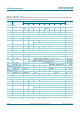
8.2.1 Register Control_1
[1] Default value.
[2] When writing to the register this bit always has to be set logic 0.
Table 6. Control_1 - control and status register 1 (address 00h) bit description
Bit Symbol Value Description Reference
7 EXT_TEST 0
[1]
normal mode Section 8.14
1 external clock test mode
6T 0
[2]
unused -
5STOP 0
[1]
RTC source clock runs Section 8.15
1 RTC clock is stopped;
RTC divider chain flip-flops are
asynchronously set logic 0;
CLKOUT at 32.768 kHz, 16.384 kHz, or
8.192 kHz is still available
4TSF1 0
[1]
no timestamp interrupt generated Section 8.12.1
1 flag set when TS input is driven to an
intermediate level between power supply
and ground;
flag must be cleared to clear interrupt
3POR_OVRD0
[1]
Power-On Reset Override (PORO) facility
disabled;
set logic 0 for normal operation
Section 8.8.2
1 Power-On Reset Override (PORO)
sequence reception enabled
2 12_24 0
[1]
24 hour mode selected Table 23
1 12 hour mode selected
1 MI 0
[1]
minute interrupt disabled Section 8.13
1 minute interrupt enabled
0SI 0
[1]
second interrupt disabled
1 second interrupt enabled