
Datasheet

PCF2127AT All information provided in this document is subject to legal disclaimers. © NXP B.V. 2013. All rights reserved.
Product data sheet Rev. 6 — 11 July 2013 4 of 86
NXP Semiconductors
PCF2127AT
Integrated RTC, TCXO and quartz crystal
7. Pinning information
7.1 Pinning
7.2 Pin description
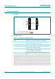
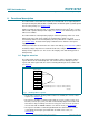
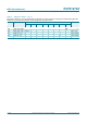
Top view. For mechanical details, see Figure 53.
Fig 2. Pin configuration for SO20 (PCF2127AT)
PCF2127AT
SCL V
DD
SDI V
BAT
SDO BBS
SDA/CE INT
IFS RST
TS PFI
CLKOUT PFO
V
SS
TEST
n.c. n.c.
n.c. n.c.
001aaj676
1
2
3
4
5
6
7
8
9
10
12
11
14
13
16
15
18
17
20
19
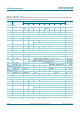
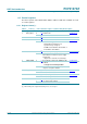
Table 4. Pin description of SO20 (PCF2127AT)
Symbol Pin Description
SCL 1 combined serial clock input for both I
2
C-bus and SPI-bus
SDI 2 serial data input for SPI-bus;
connect to pin V
SS
if I
2
C-bus is selected
SDO 3 serial data output for SPI-bus, push-pull
SDA/CE
4 combined serial data input and output for the I
2
C-bus and chip
enable input (active LOW) for the SPI-bus
IFS 5 interface selector input
connect to pin V
SS
to select the SPI-bus
connect to pin BBS to select the I
2
C-bus
TS
6 timestamp input (active LOW) with 200 k internal pull-up resistor
(R
PU
)
CLKOUT 7 clock output (open-drain)
V
SS
8 ground supply voltage
n.c. 9 to 12 not connected; do not connect; do not use as feed through
TEST 13 do not connect; do not use as feed through
PFO
14 power fail output (open-drain; active LOW)
PFI 15 power fail input
RST
16 reset output (open-drain; active LOW)
INT
17 interrupt output (open-drain; active LOW)