
Datasheet

PCF2129 All information provided in this document is subject to legal disclaimers. © NXP Semiconductors N.V. 2014. All rights reserved.
Product data sheet Rev. 7 — 19 December 2014 5 of 86
NXP Semiconductors
PCF2129
Accurate RTC with integrated quartz crystal for industrial applications
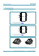
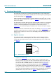
After lead forming and cutting, there remain stubs from the package assembly process.
These stubs are present at the edge of the package as illustrated in Figure 4
. The stubs
are at an electrical potential. To avoid malfunction of the PCF2129, it has to be ensured
that they are not shorted with another electrical potential (e.g. by condensation).
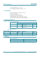
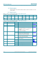
7.2 Pin description
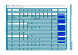
Table 4. Pin description of PCF2129
Input or input/output pins must always be at a defined level (V
SS
or V
DD
) unless otherwise specified.
Symbol Pin Description
PCF2129AT PCF2129T
SCL 1 1 combined serial clock input for both I
2
C-bus and SPI-bus
SDI 2 2 serial data input for SPI-bus
connect to pin V
SS
if I
2
C-bus is selected
SDO 3 3 serial data output for SPI-bus, push-pull
SDA/CE
4 4 combined serial data input and output for the I
2
C-bus and
chip enable input (active LOW) for the SPI-bus
IFS 5 5 interface selector input
connect to pin V
SS
to select the SPI-bus
connect to pin BBS to select the I
2
C-bus
TS
6 6 timestamp input (active LOW) with 200 k internal pull-up
resistor (R
PU
)
CLKOUT 7 7 clock output (open-drain)
V
SS
8 8 ground supply voltage
n.c. 9 to 16 9 to 12 not connected; do not connect; do not use as feed through
INT
17 13 interrupt output (open-drain; active LOW)
BBS 18 14 output voltage (battery backed)
V
BAT
19 15 battery supply voltage (backup)
connect to V
SS
if battery switch over is not used
V
DD
20 16 supply voltage