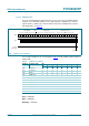
PCF85063TP Tiny Real-Time Clock/calendar Rev. 3 — 11 July 2013 Product data sheet 1. General description The PCF85063TP is a CMOS1 Real-Time Clock (RTC) and calendar optimized for low power consumption. An offset register allows fine-tuning of the clock. All addresses and data are transferred serially via the two-line bidirectional I2C-bus. Maximum bus speed is 400 kbit/s. The register address is incremented automatically after each written or read data byte. 2.
PCF85063TP NXP Semiconductors Tiny Real-Time Clock/calendar 4. Ordering information Table 1. Ordering information Type number Package PCF85063TP Name Description Version HWSON8 plastic thermal enhanced very very thin small outline package; no leads; 8 terminals; body 2 3 0.75 mm SOT1069-2 4.1 Ordering options Table 2. Ordering options Product type number IC revision Sales item (12NC) Delivery form PCF85063TP/1 1 935297365147 tape and reel, 7 inch 5. Marking Table 3.
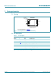
PCF85063TP NXP Semiconductors Tiny Real-Time Clock/calendar 7. Pinning information 7.1 Pinning 3&) 73 WHUPLQDO LQGH[ DUHD 26&, 9'' 26&2 &/.287 ,17 6&/ 966 6'$ DDD 7UDQVSDUHQW WRS YLHZ For mechanical details, see Figure 27. Fig 2. Pin configuration for HWSON8 (PCF85063TP) 7.2 Pin description Table 4.
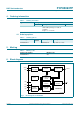
PCF85063TP NXP Semiconductors Tiny Real-Time Clock/calendar 8. Functional description The PCF85063TP contains 11 8-bit registers with an auto-incrementing register address, an on-chip 32.768 kHz oscillator with integrated capacitors, a frequency divider which provides the source clock for the Real-Time Clock (RTC) and calender, and an I2C-bus interface with a maximum data rate of 400 kbit/s.
xxxxxxxxxxxxxxxxxxxxx xxxxxxxxxxxxxxxxxxxxxxxxxx xxxxxxx x x x xxxxxxxxxxxxxxxxxxxxxxxxxxxxxx xxxxxxxxxxxxxxxxxxx xx xx xxxxx xxxxxxxxxxxxxxxxxxxxxxxxxxx xxxxxxxxxxxxxxxxxxx xxxxxx xxxxxxxxxxxxxxxxxxxxxxxxxxxxxxxxxxx xxxxxxxxxxxx x x xxxxxxxxxxxxxxxxxxxxx xxxxxxxxxxxxxxxxxxxxxxxxxxxxxx xxxxx xxxxxxxxxxxxxxxxxxxxxxxxxxxxxxxxxxxxxxxxxxxxxxxxxx xxxxxxxx xxxxxxxxxxxxxxxxxxxxxxxxx xxxxxxxxxxxxxxxxxxxx xxx NXP Semiconductors PCF85063TP Product data sheet 8.1 Registers organization Table 5.
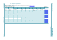
PCF85063TP NXP Semiconductors Tiny Real-Time Clock/calendar 8.2 Control registers 8.2.1 Register Control_1 Table 6. Control_1 - control and status register 1 (address 00h) bit description Bit Symbol 7 EXT_TEST 6 - 5 STOP 4 Value - 2 CIE 1 external clock test mode Section 8.2.1.1 normal mode 1 external clock test mode 0 unused - STOP bit Section 8.2.1.
PCF85063TP NXP Semiconductors Tiny Real-Time Clock/calendar From a stop condition, the first 1 second increment will take place after 32 positive edges on pin CLKOUT. Thereafter, every 64 positive edges cause a 1 second increment. Remark: Entry into test mode is not synchronized to the internal 64 Hz clock. When entering the test mode, no assumption as to the state of the prescaler can be made. Operation example: 1. Set EXT_TEST test mode (register Control_1, bit EXT_TEST = 1) 2.
PCF85063TP NXP Semiconductors Tiny Real-Time Clock/calendar Table 7. First increment of time circuits after STOP bit release Bit Prescaler bits STOP F0F1-F2 to F14 [1] 1 Hz tick Time Comment hh:mm:ss Clock is running normally 0 12:45:12 01-0 0001 1101 0100 prescaler counting normally STOP bit is activated by user.
PCF85063TP NXP Semiconductors Tiny Real-Time Clock/calendar 8.2.1.3 Software reset A reset is automatically generated at power-on. A reset can also be initiated with the software reset command. Software reset command means setting bits 6, 4, and 3 in register Control_1 (00h) logic 1 and all other bits logic 0 by sending the bit sequence 01011000 (58h), see Figure 6.
PCF85063TP NXP Semiconductors Tiny Real-Time Clock/calendar 8.2.2 Register Control_2 Table 9. Control_2 - control and status register 2 (address 01h) bit description Bit Symbol Value Description 7 to 6 - 00 unused 5 MI 4 minute interrupt 0[1] disabled 1 enabled HMI 3 half minute interrupt 0[1] disabled 1 enabled TF timer flag 0[1] no timer interrupt generated 1 2 to 0 [1] 8.2.2.1 COF[2:0] see Table 11 flag set when timer interrupt generated CLKOUT control Default value.
PCF85063TP NXP Semiconductors Tiny Real-Time Clock/calendar The duration of the timer is affected by the register Offset (see Section 8.2.3). Only when OFFSET[6:0] has the value 00h the periods are consistent. 8.2.2.2 TF: timer flag The timer flag (bit TF) is set logic 1 on the first trigger of MI or HMI and remains set until it is cleared by command. 8.2.2.3 COF[2:0]: Clock output frequency A programmable square wave is available at pin CLKOUT.
PCF85063TP NXP Semiconductors Tiny Real-Time Clock/calendar Table 12. Offset - offset register (address 02h) bit description Bit Symbol 7 MODE 6 to 0 [1] Value Description offset mode OFFSET[6:0] 0[1] normal mode: offset is made once every two hours 1 course mode: offset is made every 4 minutes offset value see Table 13 Default value. For MODE = 0, each LSB introduces an offset of 4.34 ppm. For MODE = 1, each LSB introduces an offset of 4.069 ppm. The values of 4.34 ppm and 4.
PCF85063TP NXP Semiconductors Tiny Real-Time Clock/calendar 8.2.3.1 Correction when MODE = 0 The correction is triggered once every two hours and then correction pulses are applied once per minute until the programmed correction values have been implemented. Table 14.
PCF85063TP NXP Semiconductors Tiny Real-Time Clock/calendar 8.2.3.2 Correction when MODE = 1 The correction is triggered once every four minutes and then correction pulses are applied once per second up to a maximum of 60 pulses. When correction values greater than 60 pulses are used, additional correction pulses are made in the 59th second. Clock correction is made more frequently in MODE = 1; however, this can result in higher power consumption. Table 16.
PCF85063TP NXP Semiconductors Tiny Real-Time Clock/calendar 8.2.3.3 Offset calibration workflow The calibration offset has to be calculated based on the time. Figure 8 shows the workflow how the offset register values can be calculated: 0HDVXUH WKH IUHTXHQF\ RQ SLQ &/.
PCF85063TP NXP Semiconductors Tiny Real-Time Clock/calendar GHYLDWLRQ DIWHU FRUUHFWLRQ LQ 02'( SSP GHYLDWLRQ DIWHU FRUUHFWLRQ LQ 02'( SSP PHDVXUHG FDOFXODWHG GHYLDWLRQ SSP DDD With the offset calibration an accuracy of 2 ppm (0.5 offset per LSB) can be reached (see Table 13). 1 ppm corresponds to a time deviation of 0.0864 seconds per day. (1) 3 correction pulses in MODE = 0 correspond to 13.02 ppm.
PCF85063TP NXP Semiconductors Tiny Real-Time Clock/calendar Table 20. Seconds coded in BCD format Seconds value in decimal Digit (unit place) Bit 6 Bit 3 Bit 5 Bit 4 Bit 2 Bit 1 Bit 0 00[1] 0 0 0 0 0 0 0 01 0 0 0 0 0 0 1 02 0 0 0 0 0 1 0 : : : : : : : : 09 0 0 0 1 0 0 1 10 0 0 1 0 0 0 0 : : : : : : : : 58 1 0 1 1 0 0 0 59 1 0 1 1 0 0 1 [1] 8.3.1.1 Upper-digit (ten’s place) Default value.
PCF85063TP NXP Semiconductors Tiny Real-Time Clock/calendar 8.3.2 Register Minutes Table 21. Minutes - minutes register (address 05h) bit description Bit Symbol Value Place value Description 7 - 0 - unused MINUTES 0[1] ten’s place actual minutes coded in BCD format 6 to 4 [1] to 5 0[1] to 9 3 to 0 unit place Default value. 8.3.3 Register Hours Table 22.
PCF85063TP NXP Semiconductors Tiny Real-Time Clock/calendar Table 25. Weekday assignments Day[1] Bit 2 1 0 Sunday 0 0 0 Monday 0 0 1 Tuesday 0 1 0 Wednesday 0 1 1 Thursday 1 0 0 Friday 1 0 1 Saturday[2] 1 1 0 [1] Definition may be reassigned by the user. [2] Default value. 8.3.6 Register Months Table 26.
PCF85063TP NXP Semiconductors Tiny Real-Time Clock/calendar 8.3.7 Register Years Table 28. Bit 7 to 4 Years - years register (0Ah) bit description Symbol Value Place value Description YEARS 0[1] to 9 ten’s place 0[1] to 9 unit place 3 to 0 [1] actual year coded in BCD format Default value. 8.4 Setting and reading the time Figure 11 shows the data flow and data dependencies starting from the 1 Hz clock tick.
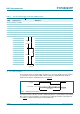
PCF85063TP NXP Semiconductors Tiny Real-Time Clock/calendar W V 67$57 6/$9( $''5(66 '$7$ '$7$ 6723 DDD Fig 12. Access time for read/write operations Because of this method, it is very important to make a read or write access in one go, that is, setting or reading seconds through to years should be made in one single access. Failing to comply with this method could result in the time becoming corrupted.
PCF85063TP NXP Semiconductors Tiny Real-Time Clock/calendar 9. Characteristics of the I2C-bus interface The I2C-bus is for bidirectional, two-line communication between different ICs or modules. The two lines are a Serial DAta line (SDA) and a Serial CLock line (SCL). Both lines must be connected to a positive supply via a pull-up resistor. Data transfer may be initiated only when the bus is not busy. 9.1 Bit transfer One data bit is transferred during each clock pulse.
PCF85063TP NXP Semiconductors Tiny Real-Time Clock/calendar MASTER TRANSMITTER/ RECEIVER SLAVE TRANSMITTER/ RECEIVER SLAVE RECEIVER MASTER TRANSMITTER/ RECEIVER MASTER TRANSMITTER SDA SCL mga807 Fig 15. System configuration 9.4 Acknowledge The number of data bytes transferred between the START and STOP conditions from transmitter to receiver is unlimited. Each byte of 8 bits is followed by an acknowledge cycle.
PCF85063TP NXP Semiconductors Tiny Real-Time Clock/calendar 9.5 I2C-bus protocol 9.5.1 Addressing One I2C-bus slave address (1010001) is reserved for the PCF85063TP. The entire I2C-bus slave address byte is shown in Table 29. Table 29. I2C slave address byte Slave address Bit 7 6 5 4 3 2 1 MSB 0 LSB 1 0 1 0 0 0 1 R/W After a START condition, the I2C slave address has to be sent to the PCF85063TP device.
PCF85063TP NXP Semiconductors Tiny Real-Time Clock/calendar DFNQRZOHGJH IURP 3&) 73 6 VODYH DGGUHVV DFNQRZOHGJH IURP 3&) 73 $ ZULWH ELW $ UHJLVWHU DGGUHVV K WR $K DFNQRZOHGJH IURP 3&) 73 6 VODYH DGGUHVV UHDG ELW $ VHW UHJLVWHU DGGUHVV 3 6723 DFNQRZOHGJH IURP PDVWHU QR DFNQRZOHGJH $ $ '$7$ %<7( /$67 '$7$ %<7( UHDG UHJLVWHU GDWD 3 WR Q GDWD E\WHV DDD DXWR LQFUHPHQW PHPRU\ UHJLVWHU DGGUHVV DXWR LQFUHPHQW PHPRU\ UHJL
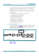
PCF85063TP NXP Semiconductors Tiny Real-Time Clock/calendar 10. Internal circuitry 3&) 73 9'' 26&, &/.287 26&2 6&/ ,17 6'$ 966 DDD Fig 19. Device diode protection diagram of PCF85063TP 11. Safety notes CAUTION This device is sensitive to ElectroStatic Discharge (ESD). Observe precautions for handling electrostatic sensitive devices. Such precautions are described in the ANSI/ESD S20.20, IEC/ST 61340-5, JESD625-A or equivalent standards.
PCF85063TP NXP Semiconductors Tiny Real-Time Clock/calendar 12. Limiting values Table 30. Limiting values In accordance with the Absolute Maximum Rating System (IEC 60134). PCF85063TP Product data sheet Symbol Parameter Conditions VDD supply voltage IDD supply current VI input voltage VO output voltage II input current at any input at any output on pins SCL, SDA, OSCI IO output current Ptot total power dissipation VESD electrostatic discharge voltage Min Max Unit 0.5 +6.
PCF85063TP NXP Semiconductors Tiny Real-Time Clock/calendar 13. Characteristics Table 31. Static characteristics VDD = 0.9 V to 5.5 V; VSS = 0 V; Tamb = 40 C to +85 C; fosc = 32.768 kHz; quartz Rs = 60 k; CL = 7 pF; unless otherwise specified. Symbol Parameter Conditions Min Typ Max Unit supply voltage interface inactive; fSCL = 0 Hz [1] 0.9 - 5.5 V interface active; fSCL = 400 kHz [1] 1.8 - 5.5 V VDD = 3.
PCF85063TP NXP Semiconductors Tiny Real-Time Clock/calendar Table 31. Static characteristics …continued VDD = 0.9 V to 5.5 V; VSS = 0 V; Tamb = 40 C to +85 C; fosc = 32.768 kHz; quartz Rs = 60 k; CL = 7 pF; unless otherwise specified. Symbol Parameter Conditions Min Typ Max Unit fosc/fosc relative oscillator frequency variation VDD = 200 mV; Tamb = 25 C - 0.075 - ppm CL(itg) integrated load capacitance on pins OSCO, OSCI CL = 7 pF 4.2 7 9.8 pF CL = 12.5 pF 7.5 12.5 17.
PCF85063TP NXP Semiconductors Tiny Real-Time Clock/calendar DDD ,'' Q$ 7HPSHUDWXUH & CL(itg) = 7 pF; CLKOUT disabled. (1) VDD = 5.5 V. (2) VDD = 3.3 V. DDD ,'' Q$ 7HPSHUDWXUH & CL(itg) = 12.5 pF; CLKOUT disabled. (1) VDD = 5.5 V. (2) VDD = 3.3 V. Fig 21.
PCF85063TP NXP Semiconductors Tiny Real-Time Clock/calendar DDD ,'' $ 9'' 9 Tamb = 25 C; fCLKOUT = 32768 Hz. (1) 47 pF CLKOUT load. (2) 22 pF CLKOUT load. DDD ,'' Q$ 9'' 9 Tamb = 25 C; CLKOUT disabled. (1) CL(itg) = 12.5 pF. (2) CL(itg) = 7 pF. Fig 22.
PCF85063TP NXP Semiconductors Tiny Real-Time Clock/calendar DDD ,'' Q$ 56 N VDD = 3.3 V; CLKOUT disabled. (1) CL(itg) = 12.5 pF; 50 C; maximum value. (2) CL(itg) = 7 pF; 50 C; maximum value. (3) CL(itg) = 12.5 pF; 25 C; typical value. (4) CL(itg) = 7 pF; 25 C; typical value. Fig 23. IDD with respect to quartz RS DDD ǻIRVF SSP 9'' 9 Tamb = 25 C. (1) CL(itg) = 7 pF.
PCF85063TP NXP Semiconductors Tiny Real-Time Clock/calendar Table 32. I2C-bus characteristics VDD = 1.8 V to 5.5 V; VSS = 0 V; Tamb = 40 C to +85 C; fosc = 32.768 kHz; quartz Rs = 60 k; CL = 7 pF; unless otherwise specified. All timing values are valid within the operating supply voltage and temperature range and referenced to VIL and VIH with an input voltage swing of VSS to VDD[1].
PCF85063TP NXP Semiconductors Tiny Real-Time Clock/calendar 14. Application information 9'' 6'$ 0$67(5 75$160,77(5 5(&(,9(5 6&/ ) Q) 9'' ,17 6&/ 26&, 26&2 9'' 3&) 73 6'$ 5 966 5 5 SXOO XS UHVLVWRU 5 6'$ 6&/ , & EXV WU &E DDD A 1 farad super capacitor combined with a low VF diode can be used as a standby or back-up supply. With the RTC in its minimum power configuration i.e. timer off and CLKOUT off, the RTC may operate for weeks. Fig 26.
PCF85063TP NXP Semiconductors Tiny Real-Time Clock/calendar 15. Package outline HWSON8: plastic thermal enhanced very very thin small outline package; no leads; 8 terminals; body 2 x 3 x 0.75 mm SOT1069-2 X B D A A2 A E A1 A3 terminal 1 index area detail X e1 terminal 1 index area e 1 4 C C A B C v w b y y1 C L K E2 8 5 D2 0 1 Dimensions Unit mm 2 mm scale A(1) A1 A2 max 0.80 0.05 0.65 nom 0.75 0.02 0.55 min 0.70 0.00 0.45 A3 b D(1) D2 E(1) E2 e e1 0.2 0.30 0.
PCF85063TP NXP Semiconductors Tiny Real-Time Clock/calendar 16. Handling information All input and output pins are protected against ElectroStatic Discharge (ESD) under normal handling. When handling Metal-Oxide Semiconductor (MOS) devices ensure that all normal precautions are taken as described in JESD625-A, IEC 61340-5 or equivalent standards. 17. Packing information 17.1 Tape and reel information 723 9,(: ' 3 : SLQ % 3 $ ' .
PCF85063TP NXP Semiconductors Tiny Real-Time Clock/calendar 18. Soldering of SMD packages This text provides a very brief insight into a complex technology. A more in-depth account of soldering ICs can be found in Application Note AN10365 “Surface mount reflow soldering description”. 18.1 Introduction to soldering Soldering is one of the most common methods through which packages are attached to Printed Circuit Boards (PCBs), to form electrical circuits.
PCF85063TP NXP Semiconductors Tiny Real-Time Clock/calendar 18.
PCF85063TP NXP Semiconductors Tiny Real-Time Clock/calendar temperature maximum peak temperature = MSL limit, damage level minimum peak temperature = minimum soldering temperature peak temperature time 001aac844 MSL: Moisture Sensitivity Level Fig 29. Temperature profiles for large and small components For further information on temperature profiles, refer to Application Note AN10365 “Surface mount reflow soldering description”.
PCF85063TP NXP Semiconductors Tiny Real-Time Clock/calendar 19. Footprint information )RRWSULQW LQIRUPDWLRQ IRU UHIORZ VROGHULQJ RI +:621 SDFNDJH 627 *[ ' 3 & Q63[ +\ 63\ *\ 6/\ %\ $\ Q63\ 63[ 6/[ VROGHU ODQG VROGHU SDVWH GHSRVLW VROGHU ODQG SOXV VROGHU SDVWH RFFXSLHG DUHD ',0(16,216 LQ PP 3 $\ %\ & ' 6/[ 6/\ 63[ 63\ *[ *\ +\ Q63[ Q63\ ,VVXH GDWH VRW BIU Fig 30.
PCF85063TP NXP Semiconductors Tiny Real-Time Clock/calendar 20. Abbreviations Table 36.
PCF85063TP NXP Semiconductors Tiny Real-Time Clock/calendar 21.
PCF85063TP NXP Semiconductors Tiny Real-Time Clock/calendar 23. Legal information 23.1 Data sheet status Document status[1][2] Product status[3] Definition Objective [short] data sheet Development This document contains data from the objective specification for product development. Preliminary [short] data sheet Qualification This document contains data from the preliminary specification. Product [short] data sheet Production This document contains the product specification.
PCF85063TP NXP Semiconductors Tiny Real-Time Clock/calendar Export control — This document as well as the item(s) described herein may be subject to export control regulations. Export might require a prior authorization from competent authorities. Non-automotive qualified products — Unless this data sheet expressly states that this specific NXP Semiconductors product is automotive qualified, the product is not suitable for automotive use.
PCF85063TP NXP Semiconductors Tiny Real-Time Clock/calendar 25. Tables Table 1. Table 2. Table 3. Table 4. Table 5. Table 6. Table 7. Table 8. Table 9. Table 10. Table 11. Table 12. Table 13. Table 14. Table 15. Table 16. Table 17. Table 18. Table 19. Table 20. Table 21. Table 22. Table 23. Table 24. Table 25. Table 26. Table 27. Table 28. Table 29. Table 30. Table 31. Table 32. Table 33. Table 34. Table 35. Table 36. Table 37. Ordering information . . . . . . . . . . . . . . . . . . . . .
PCF85063TP NXP Semiconductors Tiny Real-Time Clock/calendar 26. Figures Fig 1. Fig 2. Fig 3. Fig 4. Fig 5. Fig 6. Fig 7. Fig 8. Fig 9. Fig 10. Fig 11. Fig 12. Fig 13. Fig 14. Fig 15. Fig 16. Fig 17. Fig 18. Fig 19. Fig 20. Fig 21. Fig 22. Fig 23. Fig 24. Fig 25. Fig 26. Fig 27. Fig 28. Fig 29. Fig 30. Block diagram of PCF85063TP . . . . . . . . . . . . . . .2 Pin configuration for HWSON8 (PCF85063TP) . . .3 Handling address registers . . . . . . . . . . . . . . . . . .4 STOP bit functional diagram . . .
PCF85063TP NXP Semiconductors Tiny Real-Time Clock/calendar 27. Contents 1 2 3 4 4.1 5 6 7 7.1 7.2 8 8.1 8.2 8.2.1 8.2.1.1 8.2.1.2 8.2.1.3 8.2.2 8.2.2.1 8.2.2.2 8.2.2.3 8.2.3 8.2.3.1 8.2.3.2 8.2.3.3 8.2.4 8.3 8.3.1 8.3.1.1 8.3.2 8.3.3 8.3.4 8.3.5 8.3.6 8.3.7 8.4 9 9.1 9.2 9.3 9.4 9.5 9.5.1 9.5.2 10 11 General description . . . . . . . . . . . . . . . . . . . . . . 1 Features and benefits . . . . . . . . . . . . . . . . . . . . 1 Applications . . . . . . . . . . . . . . . . . . . . . . . . . . . .