
Datasheet

PCF85063TP All information provided in this document is subject to legal disclaimers. © NXP B.V. 2013. All rights reserved.
Product data sheet Rev. 3 — 11 July 2013 3 of 47
NXP Semiconductors
PCF85063TP
Tiny Real-Time Clock/calendar
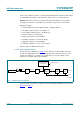
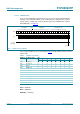
7. Pinning information
7.1 Pinning
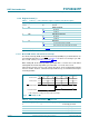
7.2 Pin description
[1] The die paddle (exposed pad) is connected to V
SS
and should be electrically isolated.
For mechanical details, see Figure 27
.
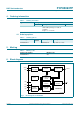
Fig 2. Pin configuration for HWSON8 (PCF85063TP)
DDD
WHUPLQDO
LQGH[DUHD
26&,
3&)73
7UDQVSDUHQWWRSYLHZ
26&2
,17
966
9''
&/.287
6&/
6'$
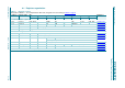
Table 4. Pin description
Symbol Pin Type Description
OSCI 1 input oscillator input
OSCO 2 output oscillator output
INT
3 output interrupt output (open-drain)
VSS 4
[1]
supply ground supply voltage
SDA 5 input/output serial data line
SCL 6 input serial clock input
CLKOUT 7 output clock output (push-pull)
VDD 8 supply supply voltage