PCF8523 Real-Time Clock (RTC) and calendar Rev. 6 — 17 September 2013 Product data sheet 1. General description The PCF8523 is a CMOS1 Real-Time Clock (RTC) and calendar optimized for low power consumption. Data is transferred serially via the I2C-bus with a maximum data rate of 1000 kbit/s. Alarm and timer functions are available with the possibility to generate a wake-up signal on an interrupt pin. An offset register allows fine-tuning of the clock.
PCF8523 NXP Semiconductors Real-Time Clock (RTC) and calendar 4. Ordering information Table 1. Ordering information Type number Package Name Description Version PCF8523T SO8 plastic small outline package; 8 leads; body width 3.9 mm SOT96-1 PCF8523TK HVSON8 plastic thermal enhanced very thin small outline package; no leads; 8 terminals; body 4 4 0.85 mm SOT909-1 PCF8523TS TSSOP14 plastic thin shrink small outline package; 14 leads; SOT402-1 body width 4.
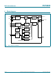
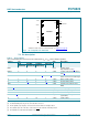
PCF8523 NXP Semiconductors Real-Time Clock (RTC) and calendar 6. Block diagram 26&, &/.287 &26&, 26&,//$725 N+] ',9,'(5 &/2&. 287 26&2 &26&2 9'' 9%$7 966 ,17 &/.287 %$77(5< %$&.83 6:,7&+ 29(5 &,5&875< &/2&. &$/,%5$7,21 2))6(7 ,17(55837 6<67(0 &21752/ 32:(5 21 5(6(7 5($/ 7,0( &/2&. 6'$ 6&/ , & %86 ,17(5)$&( $/$50 ,17 7,0(5 3&) DDD Fig 1.
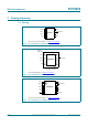
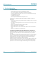
PCF8523 NXP Semiconductors Real-Time Clock (RTC) and calendar 7. Pinning information 7.1 Pinning 26&, 26&2 9'' ,17 &/.287 3&) 7 9%$7 6&/ 966 6'$ DDD Top view. For mechanical details, see Figure 39 on page 56. Fig 2. Pin configuration for SO8 (PCF8523T) WHUPLQDO LQGH[ DUHD 26&, 26&2 9'' ,17 &/.287 3&) 7. 9%$7 6&/ 966 6'$ DDD 7UDQVSDUHQW WRS YLHZ For mechanical details, see Figure 40 on page 57. Fig 3.
PCF8523 NXP Semiconductors Real-Time Clock (RTC) and calendar 26&, 26&2 3&) 8 9%$7 966 Q F ,17 9'' ,17 &/.287 Q F 6&/ 6'$ &/.287 DDD Viewed from active side. For mechanical details, see Figure 42 on page 59. Fig 5. Pin configuration for PCF8523U 7.2 Pin description Table 5. Pin description Input or input/output pins must always be at a defined level (VSS or VDD) unless otherwise specified.
PCF8523 NXP Semiconductors Real-Time Clock (RTC) and calendar 8. Functional description The PCF8523 contains: • • • • • • 20 8-bit registers with an auto-incrementing address register An on-chip 32.
PCF8523 NXP Semiconductors Real-Time Clock (RTC) and calendar 8.1 Registers overview The 20 registers of the PCF8523 are auto-incrementing after each read or write data byte up to register 13h. After register 13h, the auto-incrementing will wrap around to address 00h (see Figure 6). DGGUHVV UHJLVWHU K K K DXWR LQFUHPHQW K K K ZUDS DURXQG K Fig 6. DDD Auto-incrementing of the registers Table 6.
PCF8523 NXP Semiconductors Real-Time Clock (RTC) and calendar Table 6. Registers overview …continued Bit positions labeled as - are not implemented and will return a 0 when read. Bit T must always be written with logic 0.
PCF8523 NXP Semiconductors Real-Time Clock (RTC) and calendar 8.2 Control and status registers 8.2.1 Register Control_1 Table 7. Control_1 - control and status register 1 (address 00h) bit description Bit Symbol 7 CAP_SEL 6 5 Value Description internal oscillator capacitor selection for quartz crystals with a corresponding load capacitance 0[1] 7 pF 1 12.
PCF8523 NXP Semiconductors Real-Time Clock (RTC) and calendar 8.2.2 Register Control_2 Table 8.
PCF8523 NXP Semiconductors Real-Time Clock (RTC) and calendar 8.2.3 Register Control_3 Table 9.
PCF8523 NXP Semiconductors Real-Time Clock (RTC) and calendar 8.3 Reset A reset is automatically generated at power-on. A reset can also be initiated with the software reset command. Software reset command means setting bits 6, 4, and 3 in register Control_1 (00h) logic 1 and all other bits logic 0 by sending the bit sequence 01011000 (58h), see Figure 7.
PCF8523 NXP Semiconductors Real-Time Clock (RTC) and calendar After reset, the following mode is entered: • • • • • • • • • 32.768 kHz CLKOUT active 24 hour mode is selected Register Offset is set logic 0 No alarms set Timers disabled No interrupts enabled Battery switch-over is disabled Battery low detection is disabled 7 pF of internal oscillator capacitor selected 8.4 Interrupt function Active low interrupt signals are available at pin INT1/CLKOUT and INT2.
PCF8523 NXP Semiconductors Real-Time Clock (RTC) and calendar VHW DODUP IODJ $) $) $/$50 )/$* &/($5 6(7 WR LQWHUIDFH UHDG $) $,( IURP LQWHUIDFH FOHDU $) RIIVHW FLUFXLW DGG VXEWUDFW SXOVH IURP LQWHUIDFH FOHDU &,( VHW EDWWHU\ IODJ %6) &,( 38/6( *(1(5$725 &/($5 6(7 %6) %$77(5< )/$* 6(7 &/($5 IURP LQWHUIDFH FOHDU %6) VHW EDWWHU\ ORZ IODJ %/) %/) %$77(5< /2: )/$* 6(7 &/($5 WR LQWHUIDFH UHDG %6) %6,( WR LQWHUIDFH UHDG %/) %/,( IURP EDWWHU\ ORZ GHWHFWLRQ FLUFXLW FOHDU %/) 6,( 6(&21'
PCF8523 NXP Semiconductors Real-Time Clock (RTC) and calendar 8.5 Power management functions The PCF8523 has two power supply pins: • VDD - the main power supply input pin • VBAT - the battery backup input pin The PCF8523 has two power management functions implemented: • Battery switch-over function • Battery low detection function The power management functions are controlled by the control bits PM[2:0] in register Control_3 (02h): Table 11.
PCF8523 NXP Semiconductors Real-Time Clock (RTC) and calendar 8.5.2 Battery switch-over function The PCF8523 has a backup battery switch-over circuit. It monitors the main power supply VDD and switches automatically to the backup battery when a power failure condition is detected. One of two operation modes can be selected: • Standard mode: the power failure condition happens when: VDD < VBAT AND VDD < Vth(sw)bat • Direct switching mode: the power failure condition happens when VDD < VBAT.
PCF8523 NXP Semiconductors Real-Time Clock (RTC) and calendar 8.5.2.1 Standard mode If VDD > VBAT OR VDD > Vth(sw)bat, the internal power supply is VDD. If VDD < VBAT AND VDD < Vth(sw)bat, the internal power supply is VBAT. EDFNXS EDWWHU\ RSHUDWLRQ 9'' 9%%6 9%$7 9%%6 LQWHUQDO SRZHU VXSSO\ 9%%6 9WK VZ EDW 9 9'' 9 %6) ,17 FOHDUHG YLD LQWHUIDFH DDD Fig 9.
PCF8523 NXP Semiconductors Real-Time Clock (RTC) and calendar 8.5.2.2 Direct switching mode If VDD > VBAT the internal power supply is VDD. If VDD < VBAT the internal power supply is VBAT. The direct switching mode is useful in systems where VDD is higher than VBAT at all times (for example, VDD = 5 V, VBAT = 3.5 V). If the VDD and VBAT values are similar (for example, VDD = 3.3 V, VBAT 3.0 V), the direct switching mode is not recommended.
PCF8523 NXP Semiconductors Real-Time Clock (RTC) and calendar An unreliable battery does not ensure data integrity during periods of backup battery operation. When VBAT drops below the threshold value Vth(bat)low, the following sequence occurs (see Figure 11): 1. The battery low flag BLF is set logic 1 2. An interrupt is generated if the control bit BLIE (register Control_3) is enabled.
PCF8523 NXP Semiconductors Real-Time Clock (RTC) and calendar 8.6.1 Register Seconds Table 12. Seconds - seconds and clock integrity status register (address 03h) bit description Bit Symbol Value Place value Description 7 OS 0 - clock integrity is guaranteed 1[1] - clock integrity is not guaranteed; oscillator has stopped or been interrupted 0 to 5 ten’s place 0 to 9 unit place actual seconds coded in BCD format 6 to 4 SECONDS 3 to 0 [1] Start-up value. Table 13.
PCF8523 NXP Semiconductors Real-Time Clock (RTC) and calendar 26 DQG IODJ FDQ QRW EH FOHDUHG 26 DQG IODJ FDQ EH FOHDUHG 9'' RVFLOODWLRQ 26 IODJ 26 IODJ FOHDUHG E\ VRIWZDUH 26 IODJ VHW ZKHQ RVFLOODWLRQ VWRSV W RVFLOODWLRQ QRZ VWDEOH DDD Fig 12. OS flag 8.6.2 Register Minutes Table 14.
PCF8523 NXP Semiconductors Real-Time Clock (RTC) and calendar 8.6.5 Register Weekdays Table 17. Weekdays - weekdays register (address 07h) bit description Bit Symbol Value Description 7 to 3 - - unused 2 to 0 WEEKDAYS 0 to 6 actual weekday, values see Table 18 Table 18. Weekday assignments Day[1] Bit 2 1 0 Sunday 0 0 0 Monday 0 0 1 Tuesday 0 1 0 Wednesday 0 1 1 Thursday 1 0 0 Friday 1 0 1 Saturday 1 1 0 [1] Definition may be reassigned by the user. 8.6.
PCF8523 NXP Semiconductors Real-Time Clock (RTC) and calendar 8.6.7 Register Years Table 21. Years - years register (09h) bit description Bit Symbol Value Place value Description 7 to 4 YEARS 0 to 9 ten’s place 0 to 9 unit place 3 to 0 actual year coded in BCD format 8.6.8 Data flow of the time function Figure 13 shows the data flow and data dependencies starting from the 1 Hz clock tick. +] WLFN 6(&21'6 0,187(6 KRXU PRGH +2856 /($3 <($5 &$/&8/$7,21 '$<6 :((.
PCF8523 NXP Semiconductors Real-Time Clock (RTC) and calendar Because of this method, it is very important to make a read or write access in one go, that is, setting or reading seconds through to years should be made in one single access. Failing to comply with this method could result in the time becoming corrupted. As an example, if the time (seconds through to hours) is set in one access and then in a second access the date is set, it is possible that the time will increment between the two accesses.
PCF8523 NXP Semiconductors Real-Time Clock (RTC) and calendar 8.7.3 Register Day_alarm Table 24. Day_alarm - day alarm register (address 0Ch) bit description Bit Symbol Value Place value Description 7 AEN_D 0 - day alarm is enabled 1[1] - day alarm is disabled 6 - - - unused 5 to 4 DAY_ALARM 0 to 3 ten’s place 0 to 9 unit place day alarm information coded in BCD format 3 to 0 [1] Default value. 8.7.4 Register Weekday_alarm Table 25.
PCF8523 NXP Semiconductors Real-Time Clock (RTC) and calendar When one or several alarm registers are loaded with a valid minute, hour, day, or weekday value and its corresponding alarm enable bit (AEN_x) is logic 0, then that information is compared with the current minute, hour, day, and weekday value. When all enabled comparisons first match, the alarm flag, AF (register Control_2), is set logic 1. The generation of interrupts from the alarm function is controlled via bit AIE (register Control_1).
PCF8523 NXP Semiconductors Real-Time Clock (RTC) and calendar PLQXWH FRXQWHU PLQXWH DODUP $) ,17 6&/ LQVWUXFWLRQ &/($5 ,16758&7,21 DDD Example where only the minute alarm is used and no other interrupts are enabled. Fig 17. AF timing PCF8523 Product data sheet All information provided in this document is subject to legal disclaimers. Rev. 6 — 17 September 2013 © NXP B.V. 2013. All rights reserved.
PCF8523 NXP Semiconductors Real-Time Clock (RTC) and calendar 8.8 Register Offset The PCF8523 incorporates an offset register (address 0Eh), which can be used to implement several functions, like: • Aging adjustment • Temperature compensation • Accuracy tuning Table 28.
PCF8523 NXP Semiconductors Real-Time Clock (RTC) and calendar Table 30.
PCF8523 NXP Semiconductors Real-Time Clock (RTC) and calendar Table 32.
PCF8523 NXP Semiconductors Real-Time Clock (RTC) and calendar 0HDVXUH WKH IUHTXHQF\ RQ SLQ &/.
PCF8523 NXP Semiconductors Real-Time Clock (RTC) and calendar 8.9.1 Timer registers 8.9.1.1 Register Tmr_CLKOUT_ctrl and clock output Table 34.
PCF8523 NXP Semiconductors Real-Time Clock (RTC) and calendar 8.9.1.3 Table 35.
PCF8523 NXP Semiconductors Real-Time Clock (RTC) and calendar 8.9.1.5 Register Tmr_B_freq_ctrl Table 38. Bit Symbol Value Description 7 - - unused 6 to 4 TBW[2:0] 3 - 2 to 0 TBQ[2:0] [1] 8.9.1.6 Tmr_B_freq_ctrl - timer B frequency control register (address 12h) bit description 62.500 ms 010 78.125 ms 011 93.750 ms 100 125.000 ms 101 156.250 ms 110 187.500 ms 111 218.750 ms - unused source clock for timer B (see Table 40) 000 4.
PCF8523 NXP Semiconductors Real-Time Clock (RTC) and calendar 8.9.2 Timer A With the bit field TAC[1:0] in register Tmr_CLKOUT_ctrl (0Fh) Timer A can be configured as a countdown timer (TAC[1:0] = 01) or watchdog timer (TAC[1:0] = 10). 8.9.2.1 Watchdog timer function The 3 bits TAQ[2:0] in register Tmr_A_freq_ctrl (10h) determine one of the five source clock frequencies for the watchdog timer: 4.096 kHz, 64 Hz, 1 Hz, 1⁄60 Hz or 1⁄3600 Hz (see Table 36).
PCF8523 NXP Semiconductors Real-Time Clock (RTC) and calendar When loading the counter with 0: • The flag WTAF is reset (WTAF = 0) • Interrupt is cleared • The watchdog timer stops WTAF is read only. A read of the register Control_2 (01h) automatically resets WTAF (WTAF = 0) and clears the interrupt. 0&8 ZDWFKGRJ WLPHU YDOXH 7B$ 7B$ 7B$ :7$) ,17 DDD TAC[1:0] = 10, WTAIE = 1, WTAF = 1, an interrupt is generated. Fig 19. Watchdog activates an interrupt when timed out 8.9.2.
PCF8523 NXP Semiconductors Real-Time Clock (RTC) and calendar FRXQWGRZQ YDOXH 7B$ ;; FRXQWGRZQ FRXQWHU ;; :' &' > @ WLPHU VRXUFH FORFN &7$) ,17 7B$ 7B$ GXUDWLRQ RI ILUVW WLPHU SHULRG DIWHU HQDEOH PD\ UDQJH IURP 7B$ WR 7B$ DDD In this example, it is assumed that the countdown timer flag (CTAF) is cleared before the next countdown period expires and that the interrupt output is set to pulse mode. Fig 20.
PCF8523 NXP Semiconductors Real-Time Clock (RTC) and calendar When the interrupt generation is enabled (CTAIE = 1) and the countdown timer flag CTAF is set logic 1, an interrupt signal on INT1 is generated. The interrupt may be generated as a pulsed signal every countdown period or as a permanently active signal, which follows the condition of CTAF (register Control_2). The TAM bit (register Tmr_CLKOUT_ctrl) is used to control this mode selection.
PCF8523 NXP Semiconductors Real-Time Clock (RTC) and calendar If a new value of T_B is written before the end of the actual timer-period, this value will take immediate effect. It is not recommended to change T_B without first disabling the counter by setting TBC logic 0 (register Tmr_CLKOUT_ctrl). The update of T_B is asynchronous to the timer clock. Therefore changing it on the fly could result in a corrupted value loaded into the countdown counter.
PCF8523 NXP Semiconductors Real-Time Clock (RTC) and calendar VHFRQGV FRXQWHU PLQXWHV FRXQWHU ,17 ZKHQ 6,( HQDEOHG 6) ZKHQ 6,( HQDEOHG DDD In this example, bit TAM is set logic 1 and the SF flag is not cleared after an interrupt. Fig 22.
PCF8523 NXP Semiconductors Real-Time Clock (RTC) and calendar Table 44. Interrupt low pulse width for timer B Pulse mode, bit TBM set logic 1. Source clock (Hz). Interrupt pulse width T_B = 1[1] T_B > 1[1] 4096 122 s 244 s 64 7.812 ms see Table 38[2] 1 see Table 38 : 1⁄ 60 : : 1⁄ 3600 : : [1] T_B = loaded timer register value. Timer stops when T_B = 0. [2] If pulse period is shorter than the setting via bit TBW[2:0], the interrupt pulse width is set to 15.625 ms.
PCF8523 NXP Semiconductors Real-Time Clock (RTC) and calendar FRXQWGRZQ FRXQWHU 7B$ &7$) ,17 6&/ LQVWUXFWLRQ &/($5 ,16758&7,21 DDD (1) Indicates normal duration of INT1 pulse. The timing shown for clearing CTAF is also valid for the non-pulsed interrupt mode, that is, when TAM set logic 0, where the INT1 pulse may be shortened by setting CTAIE logic 0. Fig 25.
PCF8523 NXP Semiconductors Real-Time Clock (RTC) and calendar 8.10 STOP bit function The STOP bit function allows the accurate starting of the time circuits. The STOP bit function causes the upper part of the prescaler (F2 to F14) to be held in reset and thus no 1 Hz ticks are generated. The time circuits can then be set and do not increment until the STOP bit is released (see Figure 26).
PCF8523 NXP Semiconductors Real-Time Clock (RTC) and calendar Table 45.
PCF8523 NXP Semiconductors Real-Time Clock (RTC) and calendar 6'$ 6&/ GDWD OLQH VWDEOH GDWD YDOLG FKDQJH RI GDWD DOORZHG PEF Fig 28. Bit transfer 8.11.2 START and STOP conditions Both data and clock lines remain HIGH when the bus is not busy. A HIGH-to-LOW transition of the data line, while the clock is HIGH, is defined as the START condition (S). A LOW-to-HIGH transition of the data line, while the clock is HIGH, is defined as the STOP condition (P) (see Figure 29).
PCF8523 NXP Semiconductors Real-Time Clock (RTC) and calendar 8.11.4 Acknowledge The number of data bytes transferred between the START and STOP conditions from transmitter to receiver is unlimited. Each byte of 8 bits is followed by an acknowledge cycle.
PCF8523 NXP Semiconductors Real-Time Clock (RTC) and calendar The R/W bit defines the direction of the following single or multiple byte data transfer. For the format and the timing of the START condition (S), the STOP condition (P) and the acknowledge bit (A) refer to the I2C-bus characteristics (see Ref. 13 on page 71). In the write mode, a data transfer is terminated by sending either the STOP condition or the START condition of the next data transfer.
PCF8523 NXP Semiconductors Real-Time Clock (RTC) and calendar 10. Safety notes CAUTION This device is sensitive to ElectroStatic Discharge (ESD). Observe precautions for handling electrostatic sensitive devices. Such precautions are described in the ANSI/ESD S20.20, IEC/ST 61340-5, JESD625-A or equivalent standards. CAUTION Semiconductors are light sensitive. Exposure to light sources can cause the IC to malfunction. The IC must be protected against light.
PCF8523 NXP Semiconductors Real-Time Clock (RTC) and calendar 11. Limiting values Table 47. Limiting values In accordance with the Absolute Maximum Rating System (IEC 60134). Symbol Parameter VDD Conditions Min Max Unit supply voltage 0.5 +6.5 V IDD supply current 50 +50 mA VI input voltage 0.5 +6.5 V VO output voltage 0.5 +6.5 V II input current 10 +10 mA IO output current 10 +10 mA VBAT battery supply voltage 0.5 +6.
PCF8523 NXP Semiconductors Real-Time Clock (RTC) and calendar 12. Static characteristics Table 48. Static characteristics VDD = 1.2 V to 5.5 V; VSS = 0 V; Tamb = 40 C to +85 C; fosc = 32.768 kHz; quartz Rs = 40 k; CL = 7 pF; unless otherwise specified. Symbol Parameter Conditions Min Typ Max Unit Supplies VDD supply voltage I2C-bus inactive; for clock data integrity Tamb = 40 C to +85 C [1] 1.2 - 5.5 V Tamb = +10 C to +85 C [2] 1.0 - 5.5 V 1.6 - 5.5 V 1.8 - 5.
PCF8523 NXP Semiconductors Real-Time Clock (RTC) and calendar Table 48. Static characteristics …continued VDD = 1.2 V to 5.5 V; VSS = 0 V; Tamb = 40 C to +85 C; fosc = 32.768 kHz; quartz Rs = 40 k; CL = 7 pF; unless otherwise specified. Symbol Parameter Conditions Min Typ Max Unit on pins INT1/CLKOUT, CLKOUT, INT2, SDA (refers to external pull-up voltage) 0.5 - 5.5 V VSS - 0.
PCF8523 NXP Semiconductors Real-Time Clock (RTC) and calendar 13. Dynamic characteristics Table 49. I2C-bus interface timing All timing characteristics are valid within the operating supply voltage and ambient temperature range and reference to 30 % and 70 % with an input voltage swing of VSS to VDD (see Figure 35).
PCF8523 NXP Semiconductors Real-Time Clock (RTC) and calendar 67$57 FRQGLWLRQ 6 SURWRFRO W68 67$ ELW 06% $ W/2: ELW $ W+,*+ I ELW 5 : 6723 FRQGLWLRQ 3 DFNQRZOHGJH $ 6&/ 6&/ W%8) WI WU 6'$ W68 '$7 W+' 67$ W9' '$7 W+' '$7 W9' $&. W68 672 DDD Fig 35. I2C-bus timing diagram; rise and fall times refer to 30 % and 70 % 14. Application information 14.
PCF8523 NXP Semiconductors Real-Time Clock (RTC) and calendar • in the range of a few hundreds of A, the value of the capacitor on pin VDD must be increased to force a falling gradient of less than 0.7 V/ms on pin VDD to assure the proper functionality of the battery switch-over4 • higher than some mA it is recommended to add an RC network on the VDD pin, as shown in Figure 37:5 9'' 5 9'' ERDUG & 3&) DDD Fig 37. RC network on pin VDD A series resistor of 1 k and a capacitor of 3.
PCF8523 NXP Semiconductors Real-Time Clock (RTC) and calendar 9'' 5 6&/ 0$67(5 75$160,77(5 5(&(,9(5 6'$ & 966 9'' 26&, ,17 &/.287 &/.287 ,17 9'' 6&/ 3&) 26&2 6'$ 9%$7 966 5 5 5 SXOO XS UHVLVWRU WU 5 &E DDD R1 and C1 are recommended to limit the Slew Rate (SR, see Table 48) of VDD. If VDD drops too fast, the internal supply switch to the battery is not guaranteed. Fig 38.
PCF8523 NXP Semiconductors Real-Time Clock (RTC) and calendar 15.
PCF8523 NXP Semiconductors Real-Time Clock (RTC) and calendar +9621 SODVWLF WKHUPDO HQKDQFHG YHU\ WKLQ VPDOO RXWOLQH SDFNDJH QR OHDGV WHUPLQDOV ERG\ [ [ PP 627 PP VFDOH ; % ' $ $ ( $ F GHWDLO ; WHUPLQDO LQGH[ DUHD H WHUPLQDO LQGH[ DUHD H Y Z E 0 0 & & $ % & \ & \ / H[SRVHG WLH EDU î (K 'K ',0(16,216 PP DUH WKH RULJLQDO GLPHQVLRQV 81,7 $ PD[ $ E F ' 'K ( (K H H / Y Z \ \ PP
PCF8523 NXP Semiconductors Real-Time Clock (RTC) and calendar 76623 SODVWLF WKLQ VKULQN VPDOO RXWOLQH SDFNDJH OHDGV ERG\ ZLGWK PP ' 627 ( $ ; F \ + ( Y 0 $ = 4 $ SLQ LQGH[ $ $ $ ș / S / GHWDLO ; Z 0 E S H PP VFDOH ',0(16,216 PP DUH WKH RULJLQDO GLPHQVLRQV 81,7 $ PD[ $ $ $ E S F ' ( H + ( / / S 4 Y Z \ = ș PP
PCF8523 NXP Semiconductors Real-Time Clock (RTC) and calendar 16. Bare die outline %DUH GLH EXPSV 3&) 8 ' < ; 3& [ ( \ $ $ $ 3 3 3 3 (XURSHDQ SURMHFWLRQ GHWDLO < GHWDLO ; SFI XBGR Fig 42. Bare die outline of PCF8523U Table 50. Dimensions of PCF8523U Original dimensions are in mm. PCF8523 Product data sheet D[1] E[1] P1[2] P2[3] 0.018 - - - - 0.059 - 0.22 0.015 0.2 1.58 2.15 0.065 0.056 0.065 0.056 - - 0.
PCF8523 NXP Semiconductors Real-Time Clock (RTC) and calendar Table 51. Bump locations All x/y coordinates represent the position of the center of each bump with respect to the center (x/y = 0) of the chip; see Figure 42. Symbol Bump Coordinates (m) X Y VDD 1 714.4 911.7 OSCI 2 714.4 988.3 OSCO 3 714.4 707.3 VBAT 4 714.4 199.3 VSS 5 714.4 459.1 n.c. 6 714.4 616.7 INT2 7 714.4 895.4 CLKOUT 8 714.4 922.0 SDA 9 714.4 528.8 SCL 10 714.4 101.1 n.c.
PCF8523 NXP Semiconductors Real-Time Clock (RTC) and calendar 17. Handling information All input and output pins are protected against ElectroStatic Discharge (ESD) under normal handling. When handling Metal-Oxide Semiconductor (MOS) devices ensure that all normal precautions are taken as described in JESD625-A, IEC 61340-5 or equivalent standards. 18. Packing information 18.1 Tape and reel information 723 9,(: : % 3 $ .
PCF8523 NXP Semiconductors Real-Time Clock (RTC) and calendar Table 54. Carrier tape dimensions of PCF8523 …continued Symbol Description Value Unit SOT402-1 (TSSOP14) of PCF8523TS A0 pocket width in x direction 6.95 mm B0 pocket width in y direction 5.6 mm K0 pocket depth 1.6 mm P1 pocket hole pitch 8.0 mm W tape width in y direction 12.0 mm 18.
PCF8523 NXP Semiconductors Real-Time Clock (RTC) and calendar PP PP PP PP SODVWLN PP PHWDOO IUDPH VWUDLJKW HGJH RI WKH ZDIHU PP PP P P SODVWLF ILOP DDD Fig 46. Film Frame Carrier (FFC) (for PCF8523U) PCF8523 Product data sheet All information provided in this document is subject to legal disclaimers. Rev. 6 — 17 September 2013 © NXP B.V. 2013. All rights reserved.
PCF8523 NXP Semiconductors Real-Time Clock (RTC) and calendar 19. Soldering of SMD packages This text provides a very brief insight into a complex technology. A more in-depth account of soldering ICs can be found in Application Note AN10365 “Surface mount reflow soldering description”. 19.1 Introduction to soldering Soldering is one of the most common methods through which packages are attached to Printed Circuit Boards (PCBs), to form electrical circuits.
PCF8523 NXP Semiconductors Real-Time Clock (RTC) and calendar 19.
PCF8523 NXP Semiconductors Real-Time Clock (RTC) and calendar temperature maximum peak temperature = MSL limit, damage level minimum peak temperature = minimum soldering temperature peak temperature time 001aac844 MSL: Moisture Sensitivity Level Fig 47. Temperature profiles for large and small components For further information on temperature profiles, refer to Application Note AN10365 “Surface mount reflow soldering description”. 20.
PCF8523 NXP Semiconductors Real-Time Clock (RTC) and calendar )RRWSULQW LQIRUPDWLRQ IRU UHIORZ VROGHULQJ RI 76623 SDFNDJH 627 +[ *[ 3 +\ %\ *\ $\ & ' [ ' 3 *HQHULF IRRWSULQW SDWWHUQ 5HIHU WR WKH SDFNDJH RXWOLQH GUDZLQJ IRU DFWXDO OD\RXW VROGHU ODQG RFFXSLHG DUHD ',0(16,216 LQ PP 3 3 $\ %\ & ' ' *[ *\ +[ +\ VRW BIU Fig 49.
xxxxxxxxxxxxxxxxxxxxx xxxxxxxxxxxxxxxxxxxxxxxxxx xxxxxxx x x x xxxxxxxxxxxxxxxxxxxxxxxxxxxxxx xxxxxxxxxxxxxxxxxxx xx xx xxxxx xxxxxxxxxxxxxxxxxxxxxxxxxxx xxxxxxxxxxxxxxxxxxx xxxxxx xxxxxxxxxxxxxxxxxxxxxxxxxxxxxxxxxxx xxxxxxxxxxxx x x xxxxxxxxxxxxxxxxxxxxx xxxxxxxxxxxxxxxxxxxxxxxxxxxxxx xxxxx xxxxxxxxxxxxxxxxxxxxxxxxxxxxxxxxxxxxxxxxxxxxxxxxxx xxxxxxxx xxxxxxxxxxxxxxxxxxxxxxxxx xxxxxxxxxxxxxxxxxxxx xxx NXP Semiconductors PCF8523 Product data sheet 21. Appendix 21.1 Real-Time Clock selection Table 57.
xxxxxxxxxxxxxxxxxxxxx xxxxxxxxxxxxxxxxxxxxxxxxxx xxxxxxx x x x xxxxxxxxxxxxxxxxxxxxxxxxxxxxxx xxxxxxxxxxxxxxxxxxx xx xx xxxxx xxxxxxxxxxxxxxxxxxxxxxxxxxx xxxxxxxxxxxxxxxxxxx xxxxxx xxxxxxxxxxxxxxxxxxxxxxxxxxxxxxxxxxx xxxxxxxxxxxx x x xxxxxxxxxxxxxxxxxxxxx xxxxxxxxxxxxxxxxxxxxxxxxxxxxxx xxxxx xxxxxxxxxxxxxxxxxxxxxxxxxxxxxxxxxxxxxxxxxxxxxxxxxx xxxxxxxx xxxxxxxxxxxxxxxxxxxxxxxxx xxxxxxxxxxxxxxxxxxxx xxx Selection of Real-Time Clocks …continued Rev.
PCF8523 NXP Semiconductors Real-Time Clock (RTC) and calendar 22. Abbreviations Table 58.
PCF8523 NXP Semiconductors Real-Time Clock (RTC) and calendar 23.
PCF8523 NXP Semiconductors Real-Time Clock (RTC) and calendar 24. Revision history Table 59. Revision history Document ID Release date Data sheet status Change notice Supersedes PCF8523 v.6 20130917 Product data sheet - PCF8523 v.5 Modifications: • • • • • Added Section 14.1 Added description of Table 5 Added Section 21 Improved Figure 8 Adjusted Section 8.5.2.3 PCF8523 v.5 20130318 Product data sheet - PCF8523 v.4 PCF8523 v.4 20120705 Product data sheet - PCF8523 v.3 PCF8523 v.
PCF8523 NXP Semiconductors Real-Time Clock (RTC) and calendar 25. Legal information 25.1 Data sheet status Document status[1][2] Product status[3] Definition Objective [short] data sheet Development This document contains data from the objective specification for product development. Preliminary [short] data sheet Qualification This document contains data from the preliminary specification. Product [short] data sheet Production This document contains the product specification.
PCF8523 NXP Semiconductors Real-Time Clock (RTC) and calendar Export control — This document as well as the item(s) described herein may be subject to export control regulations. Export might require a prior authorization from competent authorities. Non-automotive qualified products — Unless this data sheet expressly states that this specific NXP Semiconductors product is automotive qualified, the product is not suitable for automotive use.
PCF8523 NXP Semiconductors Real-Time Clock (RTC) and calendar 27. Tables Table 1. Table 2. Table 3. Table 4. Table 5. Table 6. Table 7. Table 8. Table 9. Table 10. Table 11. Table 12. Table 13. Table 14. Table 15. Table 16. Table 17. Table 18. Table 19. Table 20. Table 21. Table 22. Table 23. Table 24. Table 25. Table 26. Table 27. Table 28. Table 29. Table 30. Table 31. Table 32. Table 33. Table 34. Table 35. Table 36. Table 37. Table 38. Ordering information . . . . . . . . . . . . . . . . . . . . .
PCF8523 NXP Semiconductors Real-Time Clock (RTC) and calendar 28. Figures Fig 1. Fig 2. Fig 3. Fig 4. Fig 5. Fig 6. Fig 7. Fig 8. Fig 9. Fig 10. Fig 11. Fig 12. Fig 13. Fig 14. Fig 15. Fig 16. Fig 17. Fig 18. Fig 19. Fig 20. Fig 21. Fig 22. Fig 23. Fig 24. Fig 25. Fig 26. Fig 27. Fig 28. Fig 29. Fig 30. Fig 31. Fig 32. Fig 33. Fig 34. Fig 35. Fig 36. Fig 37. Fig 38. Fig 39. Fig 40. Fig 41. Fig 42. Fig 43. Fig 44. Fig 45. Fig 46. Fig 47. Block diagram of PCF8523 . . . . . . . . . . . . . . . . . .
PCF8523 NXP Semiconductors Real-Time Clock (RTC) and calendar 29. Contents 1 2 3 4 4.1 5 6 7 7.1 7.2 8 8.1 8.2 8.2.1 8.2.2 8.2.3 8.3 8.4 8.5 8.5.1 8.5.2 8.5.2.1 8.5.2.2 8.5.2.3 General description . . . . . . . . . . . . . . . . . . . . . . 1 Features and benefits . . . . . . . . . . . . . . . . . . . . 1 Applications . . . . . . . . . . . . . . . . . . . . . . . . . . . . 1 Ordering information . . . . . . . . . . . . . . . . . . . . . 2 Ordering options . . . . . . . . . . . . . . . . . . . . . . . .
PCF8523 NXP Semiconductors Real-Time Clock (RTC) and calendar 22 23 24 25 25.1 25.2 25.3 25.4 26 27 28 29 Abbreviations . . . . . . . . . . . . . . . . . . . . . . . . . . References . . . . . . . . . . . . . . . . . . . . . . . . . . . . Revision history . . . . . . . . . . . . . . . . . . . . . . . . Legal information. . . . . . . . . . . . . . . . . . . . . . . Data sheet status . . . . . . . . . . . . . . . . . . . . . . Definitions . . . . . . . . . . . . . . . . . . . . . . . . . . . .