
Datasheet

PCF8523 All information provided in this document is subject to legal disclaimers. © NXP B.V. 2013. All rights reserved.
Product data sheet Rev. 6 — 17 September 2013 5 of 78
NXP Semiconductors
PCF8523
Real-Time Clock (RTC) and calendar
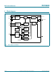
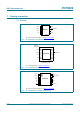
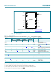
7.2 Pin description
[1] Wire length between quartz and package should be minimized.
[2] For manufacturing tests only; do not connect it and do not use it.
[3] The die paddle (exposed pad) is connected to V
SS
and should be electrically isolated.
[4] The substrate (rear side of the die) is connected to V
SS
and should be electrically isolated.
[5] The PCF8523 can either drive the CLKOUT or the INT1
.
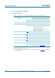
Viewed from active side. For mechanical details, see Figure 42 on page 59
.
Fig 5. Pin configuration for PCF8523U
DDD
3&)8
9
''
26&,
26&2
9
%$7
9
66
,17
QF
&/.287
6'$
6&/
QF
,17&/.287
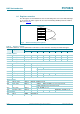
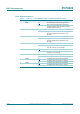
Table 5. Pin description
Input or input/output pins must always be at a defined level (V
SS
or V
DD
) unless otherwise specified.
Symbol Pin Type Description
SO8
(PCF8523T)
HVSON8
(PCF8523TK)
TSSOP14
(PCF8523TS)
PCF8523U
OSCI 1 1 1 2 input oscillator input;
high-impedance node
[1]
OSCO 2 2 2 3 output oscillator output; high-impedance
node
[1]
n.c. - - 3, 6, 9, 12
[2]
6 and 11
[2]
- not connected; do not connect
and do not use it as feed through
V
BAT
3 3 4 4 supply battery supply voltage
V
SS
44
[3]
55
[4]
supply ground supply voltage
INT2
- - 7 7 output interrupt 2 (open-drain, active
LOW)
CLKOUT
[5]
- - 8 8 output clock output (open-drain)
SDA 5 5 10 9 input/output serial data input/output
SCL 6 6 11 10 input serial clock input
INT1
/CLKOUT
[5]
7 7 13 12 output interrupt 1/clock output
(open-drain)
V
DD
8 8 14 1 supply supply voltage