
Datasheet


PCF8563 All information provided in this document is subject to legal disclaimers. © NXP B.V. 2012. All rights reserved.
Product data sheet Rev. 10 — 3 April 2012 4 of 50
NXP Semiconductors
PCF8563
Real-time clock/calendar
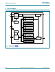
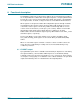
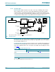
7. Pinning information
7.1 Pinning
For mechanical details, see Figure 30. Top view. For mechanical details, see
Figure 31
.
Fig 2. Pin configuration for HVSON10
(PCF8563BS)
Fig 3. Pin configuration for DIP8
(PCF8563P)
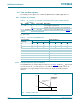
Top view. For mechanical details, see
Figure 32
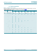
.
Top view. For mechanical details, see
Figure 33.
Fig 4. Pin configuration for SO8
(PCF8563T)
Fig 5. Pin configuration for TSSOP8
(PCF8563TS)
001aaf981
PCF8563BS
SDA
INT
V
SS
SCL
n.c. CLKOUT
OSCO V
DD
OSCI n.c.
Transparent top view
5
6
4 7
3 8
2 9
1 10
terminal 1
index area
PCF8563P
OSCI
V
DD
OSCO
CLKOUT
INT
SCL
V
SS
SDA
001aaf977
1
2
3
4
6
5
8
7
PCF8563T
OSCI V
DD
OSCO CLKOUT
INT
SCL
V
SS
SDA
001aaf975
1
2
3
4
6
5
8
7
PCF8563TS
OSCI V
DD
OSCO CLKOUT
INT SCL
V
SS
SDA
001aaf976
1
2
3
4
6
5
8
7