
Datasheet


PCF8563 All information provided in this document is subject to legal disclaimers. © NXP B.V. 2012. All rights reserved.
Product data sheet Rev. 10 — 3 April 2012 6 of 50
NXP Semiconductors
PCF8563
Real-time clock/calendar
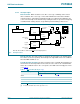
8. Functional description
The PCF8563 contains sixteen 8-bit registers with an auto-incrementing register address,
an on-chip 32.768 kHz oscillator with one integrated capacitor, a frequency divider which
provides the source clock for the Real-Time Clock (RTC) and calender, a programmable
clock output, a timer, an alarm, a voltage-low detector, and a 400 kHz I
2
C-bus interface.
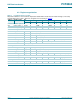
All 16 registers are designed as addressable 8-bit parallel registers although not all bits
are implemented. The first two registers (memory address 00h and 01h) are used as
control and/or status registers. The memory addresses 02h through 08h are used as
counters for the clock function (seconds up to years counters). Address locations 09h
through 0Ch contain alarm registers which define the conditions for an alarm.
Address 0Dh controls the CLKOUT output frequency. 0Eh and 0Fh are the Timer_control
and Timer registers, respectively.
The Seconds, Minutes, Hours, Days, Months, Years as well as the Minute_alarm,
Hour_alarm, and Day_alarm registers are all coded in Binary Coded Decimal (BCD)
format.
When one of the RTC registers is written or read, the contents of all time counters are
frozen. Therefore, faulty writing or reading of the clock and calendar during a carry
condition is prevented.
8.1 CLKOUT output
A programmable square wave is available at the CLKOUT pin. Operation is controlled by
the register CLKOUT_control at address 0Dh. Frequencies of 32.768 kHz (default),
1.024 kHz, 32 Hz, and 1 Hz can be generated for use as a system clock, microcontroller
clock, input to a charge pump, or for calibration of the oscillator. CLKOUT is an open-drain
output and enabled at power-on. If disabled it becomes high-impedance.