
Datasheet


PCF8563 All information provided in this document is subject to legal disclaimers. © NXP B.V. 2012. All rights reserved.
Product data sheet Rev. 10 — 3 April 2012 8 of 50
NXP Semiconductors
PCF8563
Real-time clock/calendar
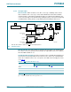
8.3 Control registers
8.3.1 Register Control_status_1
[1] Default value.
[2] Bits labeled as N should always be written with logic 0.
8.3.2 Register Control_status_2
[1] Bits labeled as N should always be written with logic 0.
[2] Default value.
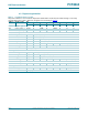
Table 5. Control_status_1 - control and status register 1 (address 00h) bit description
Bit Symbol Value Description Reference
7 TEST1 0
[1]
normal mode
must be set to logic 0 during normal operations
Section 8.9
1 EXT_CLK test mode
6N 0
[2]
unused
5STOP0
[1]
RTC source clock runs Section 8.10
1 all RTC divider chain flip-flops are asynchronously set to logic 0; the RTC
clock is stopped (CLKOUT at 32.768 kHz is still available)
4N 0
[2]
unused
3 TESTC 0 Power-On Reset (POR) override facility is disabled; set to logic 0 for
normal operation
Section 8.11.1
1
[1]
Power-On Reset (POR) override may be enabled
2to0 N 000
[2]
unused
Table 6. Control_status_2 - control and status register 2 (address 01h) bit description
Bit Symbol Value Description Reference
7to5 N 000
[1]
unused
4TI_TP0
[2]
INT is active when TF is active (subject to the status of TIE) Section 8.3.2.1
and
Section 8.8
1INT pulses active according to Table 7 (subject to the status of TIE);
Remark: note that if AF and AIE are active then INT will be
permanently active
3AF 0
[2]
read: alarm flag inactive Section 8.3.2.1
write: alarm flag is cleared
1 read: alarm flag active
write: alarm flag remains unchanged
2TF 0
[2]
read: timer flag inactive
write: timer flag is cleared
1 read: timer flag active
write: timer flag remains unchanged
1AIE 0
[2]
alarm interrupt disabled
1 alarm interrupt enabled
0TIE 0
[2]
timer interrupt disabled
1 timer interrupt enabled