INTEGRATED CIRCUITS DATA SHEET TDA8560Q 2 × 40 W/2 Ω stereo BTL car radio power amplifier with diagnostic facility Product specification Supersedes data of March 1994 File under Integrated Circuits, IC01 1996 Jan 08
Philips Semiconductors Product specification 2 × 40 W/2 Ω stereo BTL car radio power amplifier with diagnostic facility TDA8560Q FEATURES • Thermally protected • Requires very few external components • Reverse polarity safe • High output power • Electrostatic discharge protection • 4 Ω and 2 Ω load impedance • No switch-on/switch-off plop • Low output offset voltage • Flexible leads • Fixed gain • Low thermal resistance.
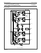
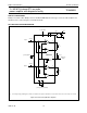
Philips Semiconductors Product specification 2 × 40 W/2 Ω stereo BTL car radio power amplifier with diagnostic facility TDA8560Q BLOCK DIAGRAM V P1 3 input 1 1 mute switch VP2 10 Cm TDA8560Q 4 VA 365 Ω 18 kΩ power stage mute switch Cm PROTECTIONS Load dump Soar Thermal Short - circuit Reverse polarity 6 VA 30 kΩ output 1A output 1B 365 Ω 18 kΩ power stage VP 11 stand-by switch mode switch stand-by reference voltage VA 15 kΩ x1 mute switch DIAGNOSTIC INTERFACE 12 diagnostic output 1
Philips Semiconductors Product specification 2 × 40 W/2 Ω stereo BTL car radio power amplifier with diagnostic facility PINNING TDA8560Q FUNCTIONAL DESCRIPTION SYMBOL PIN The TDA8560Q contains two identical amplifiers and can be used for bridge applications. The gain of each amplifier is fixed at 40 dB. Special features of the device are as follows.
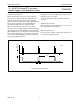
Philips Semiconductors Product specification 2 × 40 W/2 Ω stereo BTL car radio power amplifier with diagnostic facility TDA8560Q During this short-circuit condition, pin 12 is low for 20 ms and high for 50 µs (see Fig.4).
Philips Semiconductors Product specification 2 × 40 W/2 Ω stereo BTL car radio power amplifier with diagnostic facility TDA8560Q LIMITING VALUES In accordance with the Absolute Maximum Rating System (IEC 134). SYMBOL PARAMETER CONDITIONS MIN. MAX. UNIT supply voltage VP − operating non-operating during 50 ms; tr ≥ 2.
Philips Semiconductors Product specification 2 × 40 W/2 Ω stereo BTL car radio power amplifier with diagnostic facility TDA8560Q DC CHARACTERISTICS VP = 14.4 V; Tamb = 25 °C; measured in Fig.6; unless otherwise specified. SYMBOL PARAMETER CONDITIONS MIN. TYP. MAX. UNIT Supply VP supply voltage note 1 6.0 14.4 18 V Iq quiescent current RL = ∞ − 115 180 mA 8.5 − VP V − 15 40 µA Operating condition V11 mode switch voltage level I11 mode switch current V11 = 14.
Philips Semiconductors Product specification 2 × 40 W/2 Ω stereo BTL car radio power amplifier with diagnostic facility TDA8560Q AC CHARACTERISTICS VP = 14.4 V; RL = 2 Ω; f = 1 kHz; Tamb = 25 °C; measured in Fig.6; unless otherwise specified. SYMBOL Po Po THD PARAMETER output power output power total harmonic distortion CONDITIONS MIN. TYP. MAX. UNIT THD = 0.5% 25 30 − W THD = 10% 33 40 − W THD = 30% 45 55 − W THD = 0.5% − 25 − W THD = 10% − 35 − W VP = 13.
Philips Semiconductors Product specification 2 × 40 W/2 Ω stereo BTL car radio power amplifier with diagnostic facility TDA8560Q AC CHARACTERISTICS VP = 14.4 V; RL = 4 Ω; f = 1 kHz; Tamb = 25 °C; measured in Fig.6; unless otherwise specified. SYMBOL Po Po THD 1996 Jan 08 PARAMETER output power output power total harmonic distortion CONDITIONS MIN. TYP. MAX. UNIT THD = 0.5% 16 19 − W THD = 10% 21 25 − W THD = 30% 28 35 − W THD = 0.
Philips Semiconductors Product specification 2 × 40 W/2 Ω stereo BTL car radio power amplifier with diagnostic facility TDA8560Q QUALITY SPECIFICATION Quality in accordance with “Quality reference handbook SNW-FQ-611E”, if this type used as an audio amplifier. This handbook can be ordered using the code 9397 750 00192. TEST AND APPLICATION INFORMATION mode switch VP 11 470 nF input 1 3 14.
Philips Semiconductors Product specification 2 × 40 W/2 Ω stereo BTL car radio power amplifier with diagnostic facility TDA8560Q Diagnostic output handbook, halfpage Special care must be taken in the printed-circuit board layout to separate pin 12 from pin 1 and pin 13, to minimize the crosstalk between the diagnostic output and the inputs.
Philips Semiconductors Product specification 2 × 40 W/2 Ω stereo BTL car radio power amplifier with diagnostic facility TDA8560Q MGA905 70 o (W) 60 handbook, P full pagewidth 50 (1) 40 (2) 30 (3) 20 10 0 8 10 12 14 16 VP (V) 18 (1) THD = 30%. (2) THD = 10%. (3) THD = 0.5%. Fig.9 Output power as a function of supply voltage; f = 1 kHz; RL = 2 Ω. MGA906 33 Po (W) 31 29 27 25 23 10 10 2 10 3 10 4 f (Hz) Fig.10 Output power as a function of frequency; THD = 0.5%; VP = 14.
Philips Semiconductors Product specification 2 × 40 W/2 Ω stereo BTL car radio power amplifier with diagnostic facility TDA8560Q MGA907 1 THD (%) (1) 10 1 (2) (3) 10 2 10 10 2 10 3 10 4 10 5 f (Hz) (1) Po = 0.1 W. (2) Po = 1 W. (3) Po = 10 W. Fig.11 Total harmonic distortion as a function of frequency; VP = 14.4 V; RL = 2 Ω. MGA908 30 SVRR (dB) 40 (1) 50 (2) 60 70 80 10 10 2 10 3 10 4 f (Hz) (1) On condition. (2) Mute condition. Fig.
Philips Semiconductors Product specification 2 × 40 W/2 Ω stereo BTL car radio power amplifier with diagnostic facility TDA8560Q MGA910 30 α cs (dB) 40 50 60 70 80 10 10 2 10 3 10 4 f (Hz) 10 5 Fig.13 Channel separation as a function of frequency; VP = 14.4 V; Po = 25 W; RL = 2 Ω; Rs = 10 kΩ. MGA909 150 handbook, full pagewidth Iq (mA) 130 110 90 70 50 8 10 12 14 16 Fig.14 Quiescent current as a function of supply voltage; RL = ∞.
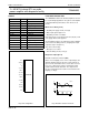
Philips Semiconductors Product specification 2 × 40 W/2 Ω stereo BTL car radio power amplifier with diagnostic facility TDA8560Q PACKAGE OUTLINE DBS13P: plastic DIL-bent-SIL power package; 13 leads (lead length 12 mm) SOT141-6 non-concave Dh x D Eh view B: mounting base side d A2 B j E A L3 L Q c 1 13 e1 Z e e2 m w M bp 0 5 v M 10 mm scale DIMENSIONS (mm are the original dimensions) UNIT A A2 bp c D (1) d Dh E (1) e e1 e2 Eh j L L3 m Q v w x Z (1) mm 17.
Philips Semiconductors Product specification 2 × 40 W/2 Ω stereo BTL car radio power amplifier with diagnostic facility TDA8560Q The device may be mounted up to the seating plane, but the temperature of the plastic body must not exceed the specified maximum storage temperature (Tstg max). If the printed-circuit board has been pre-heated, forced cooling may be necessary immediately after soldering to keep the temperature within the permissible limit.