TDA8752B Triple high-speed Analog-to-Digital Converter 110 Msps Rev. 03 — 21 July 2000 Product specification 1. General description The TDA8752B is a triple 8-bit ADC with controllable amplifiers and clamps for the digitizing of large bandwidth RGB signals. The clamp level, the gain and all other settings are controlled via a serial interface (either I2C-bus or 3-wire serial bus, selected via a logic input).
TDA8752B Philips Semiconductors Triple high-speed Analog-to-Digital Converter 110 Msps ■ Power-down mode ■ Possibility to use up to four ICs in the same system when using the I2C-bus interface, or more when using the 3-wire serial bus interface ■ 1.1 W power dissipation. 3. Applications ■ ■ ■ ■ ■ RGB high-speed digitizing LCD panels drive LCD projection systems VGA and higher resolutions Using two ICs in parallel, a higher display resolution can be obtained: 200 MHz pixel frequency. 4.
TDA8752B Philips Semiconductors Triple high-speed Analog-to-Digital Converter 110 Msps Table 1: Quick reference data…continued Symbol Parameter Conditions DRPLL PLL divider ratio Ptot total power dissipation jPLL(rms) maximum PLL phase jitter (RMS value) Min Typ Max Unit 100 − 4095 fclk = 110 MHz; ramp input − 1.1 − W fref = 66.67 kHz; fclk = 110 MHz − 112 − ps 5.
TDA8752B Philips Semiconductors Triple high-speed Analog-to-Digital Converter 110 Msps 6.
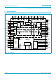
TDA8752B Philips Semiconductors Triple high-speed Analog-to-Digital Converter 110 Msps CLP RCLP RAGC CLAMP CONTROL VP DAC 150 kΩ RIN CLKADC 8 MUX Vref ADC AGC REGISTER I2C-bus: 8 bits (Or) VCCAR 3 kΩ ROR OUTPUTS 8 R0 to R7 8 45 kΩ D DAC OE D≥R R 5 1 8 RBOT 7 REGISTER FINE GAIN ADJUST 1 I2C-bus: 5 bits (Fr) REGISTER COARSE GAIN ADJUST I2C-bus: 7 bits (Cr) I2C-BUS FCE468 RGAINC HSYNCI Fig 2. Red channel diagram. © Philips Electronics N.V. 2000. All rights reserved.
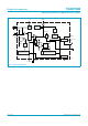
TDA8752B Philips Semiconductors Triple high-speed Analog-to-Digital Converter 110 Msps CP CZ COAST CZ CKEXT INV MUX 0°/180° CP I2C-bus; 1 bit (Vlevel) CKREF PHASE FREQUENCY edge selector DETECTOR I2C-bus; 1 bit I2C-bus; 5 bits (Edge) (Ip, Up, Do) 12 to 100 MHz loop filter I2C-bus; 3 bits (Z) VCO I2C-bus; phase selector A 2 bits (Vco) I2C-bus; I2C-bus; 5 bits (Pa) 1 bit (Cka) CLKADC MUX DIV N (100 to 4095) I2C-bus; 12 bits (Di) CKADCO CKBO I2C-bus; 1 bit (Ckb) phase selector B I2C-bus; 5
TDA8752B Philips Semiconductors Triple high-speed Analog-to-Digital Converter 110 Msps 7. Pinning information 82 OGNDPLL 81 CKAO 83 CKBO 85 VCCO(PLL) 84 CKADCO 86 DGND 87 OE 88 PWDWN 89 CLP 90 HSYNC 91 INV 92 CKEXT 93 COAST 94 CKREF 96 AGNDPLL 95 VCCD 97 CP 99 VCCA(PLL) 98 CZ 100 n.c. 7.1 Pinning n.c. 1 80 CKREFO DEC2 2 Vref DEC1 3 79 VCCO(R) 78 R7 4 77 R6 n.c.
TDA8752B Philips Semiconductors Triple high-speed Analog-to-Digital Converter 110 Msps 7.2 Pin description Table 3: Pin description Symbol Pin Description n.c. 1 not connected DEC2 2 main regulator decoupling input 2 Vref 3 gain stabilizer voltage reference input DEC1 4 main regulator decoupling input 1 n.c.
TDA8752B Philips Semiconductors Triple high-speed Analog-to-Digital Converter 110 Msps Table 3: Pin description…continued Symbol Pin Description SDA 39 I2C-bus/3-wire serial bus data input VDDD 40 logic I2C-bus/3-wire serial bus digital power supply VSSD 41 logic I2C-bus/3-wire serial bus digital ground SCL 42 I2C-bus/3-wire serial bus clock input n.c. 43 not connected n.c.
TDA8752B Philips Semiconductors Triple high-speed Analog-to-Digital Converter 110 Msps Table 3: Pin description…continued Symbol Pin Description CKREFO 80 reference output clock re-synchronized horizontal pulse CKAO 81 PLL clock output 3 (in phase with reference output clock CKAO or CKBO) OGNDPLL 82 PLL digital ground CKBO 83 PLL clock output 2 CKADCO 84 PLL clock output 1 (in phase with internal ADC clock) VCCO(PLL) 85 PLL output power supply DGND 86 digital ground OE 87 outp
TDA8752B Philips Semiconductors Triple high-speed Analog-to-Digital Converter 110 Msps 8. Functional description This triple high-speed 8-bit ADC is designed to convert RGB signals, coming from an analog source, into digital data used by a LCD driver (pixel clock up to 200 MHz when using 2 ICs). 8.1 IC analog video inputs The video inputs are internally DC polarized. These inputs are AC coupled externally. 8.
TDA8752B Philips Semiconductors Triple high-speed Analog-to-Digital Converter 110 Msps The calibration of the gains is done using the following principle. From the reference voltage Vref a reference signal of 0.156 V (p-p) (1⁄16Vref) is generated internally. During the synchronization part of the video line, the multiplexer, controlled by the TTL synchronization signal (HSYNCI, coming from HSYNC; see Figure 1) with a width equal to one of the video synchronization signals (e.g.
TDA8752B Philips Semiconductors Triple high-speed Analog-to-Digital Converter 110 Msps ADC output code GNCOARSE 255 G(max) G(min) 227 coarse register value (67 codes) NCOARSE 160 128 NFINE = 0 NFINE = 31 Vref FCE473 Fig 7. Fine gain correction for a coarse gain GNCOARSE. 8.4 ADCs The ADCs are 8-bit with a maximum clock frequency of 110 Msps. The ADCs input range is 1 V (p-p) full-scale. One out of range bit exists per channel (ROR, GOR and BOR).
TDA8752B Philips Semiconductors Triple high-speed Analog-to-Digital Converter 110 Msps Where: fn = the natural PLL frequency KO = the VCO gain DR = PLL divider ratio CZ and CP = capacitors of the PLL filter. The other PLL equation is as follows: 1 1 fn f z = ------------------------------ and ξ = --- × ----- 2π × R × C Z 2 f z (2) Where: fz = loop filter zero frequency R = the chosen resistance for the filter ξ = the damping factor FO = 0 dB loop gain frequency.
TDA8752B Philips Semiconductors Triple high-speed Analog-to-Digital Converter 110 Msps The PLL can be used in three different methods: • The IC can be used as stand-alone with a sampling frequency of up to 110 MHz.
TDA8752B Philips Semiconductors Triple high-speed Analog-to-Digital Converter 110 Msps COAST CKEXT INV 12 to 100 MHz MUX CKADCO 0 /180 phase selector A I2C-bus; I2C-bus; 5 bits (Pa) 1 bit (Cka) (Cka = 1) CLKADC CKBO MUX CKREF PLL I2C-bus; 1 bit (Ckb) (Ckb = 1) phase selector B I2C-bus; 5 bits (Pb) NCKBO CKAO MUX Master TDA8752B (even pixels) I2C-bus; 1 bit (Ckab) (Ckab = 1) SYNCHRO CKEXT COAST CKREFO INV 12 to 100 MHz MUX CKADCO 0 /180 phase selector A I2C-bus; I2C-bus; 5 bits (Pa)
TDA8752B Philips Semiconductors Triple high-speed Analog-to-Digital Converter 110 Msps 9. I2C-bus and 3-wire serial bus interfaces 9.1 Register definitions The configuration of the different registers is shown in Table 4.
TDA8752B Philips Semiconductors Triple high-speed Analog-to-Digital Converter 110 Msps Table 5: Coding Programmed code Clamp code ADC output 0 −63.5 underflow 1 −63 2 −62.5 ... ... 127 0 0 ... ... ... 254 63.5 63 or 64 255 64 64 256 120 120 ... ... ... 287 136 136 The default programmed value is: • Programmed code = 127 • Clamp code = 0 • ADC output = 0. 9.1.
TDA8752B Philips Semiconductors Triple high-speed Analog-to-Digital Converter 110 Msps Table 7: Gain correspondence (FINE) NFINE Gain Vi to be full-scale (V) 0 0.825 1.212 31 0.878 1.139 The default programmed value is: NFINE = 0. 9.1.3 Control register COAST and HSYNC signals can be inverted by setting the I2C-bus control bits ‘Vlevel’ and ‘Hlevel’ respectively. When ‘Vlevel’ and ‘Hlevel’ are set to zero respectively, COAST and HSYNC are active HIGH.
TDA8752B Philips Semiconductors Triple high-speed Analog-to-Digital Converter 110 Msps Table 9: VCO register bits Z2 Z1 Z0 Resistance (kΩ) 0 0 0 high impedance 0 0 1 128 0 1 0 32 0 1 1 16 1 0 0 8 1 0 1 4 1 1 0 2 1 1 1 1 Table 10: VCO gain control Vco1 Vco0 VCO gain (MHz/V) Pixel clock frequency range (MHz) 0 0 15 10 to 20 0 1 20 20 to 40 1 0 35 40 to 70 1 1 50 70 to 110 The bits Vco1 and Vco0 control the VCO gain.
TDA8752B Philips Semiconductors Triple high-speed Analog-to-Digital Converter 110 Msps 9.1.5 Divider register This register controls the PLL frequency. The bits are the LSB bits. The default programmed value is 0011 0010 0000 = 800. The MSB bits (Di11, Di10 and Di9) and the LSB bit (Di0) have to be programmed before bits ‘Di8’ to ‘Di1’ are programmed, to obtain the required divider ratio.
TDA8752B Philips Semiconductors Triple high-speed Analog-to-Digital Converter 110 Msps 9.2 I2C-bus protocol Table 12: I2C-bus address A7 A6 A5 A4 A3 A2 A1 A0 1 0 0 1 1 ADD2 ADD1 0 The I2C-bus address of the circuit is 1001 1xx0. Bits ‘A2’ and ‘A1’ are fixed by the potential on pins ADD1 and ADD2. Thus, four TDA8752Bs can be used on the same system, using the addresses for ADD1 and ADD2 with the I2C-bus.
Philips Semiconductors 9397 750 07338 Product specification 9.3 3-wire serial bus protocol For the 3-wire serial bus the first byte refers to the register address which is programmed. The second byte refers to the data to be sent to the chosen register (see Table 4). The acquisition is achieved via SEN. Using the 3-wire serial bus interface, an indefinite number of ICs can operate on the same system. Pin SEN is used to validate the circuits.
TDA8752B Philips Semiconductors Triple high-speed Analog-to-Digital Converter 110 Msps 10. Limiting values Table 15: Limiting values In accordance with the Absolute Maximum Rating System (IEC 60134). Symbol Parameter VCCA Conditions Min Max Unit analog supply voltage −0.3 +7.0 V VCCD digital supply voltage −0.3 +7.0 V VDDD logic supply voltage −0.3 +7.0 V VCCO output stages supply voltage −0.3 +7.0 V ∆VCC supply voltage differences VCCA − VCCD −1.0 +1.
TDA8752B Philips Semiconductors Triple high-speed Analog-to-Digital Converter 110 Msps Table 17: Characteristics…continued VCCA = V11 (or V19, V27 or V99) referenced to AGND (V13, V21, V29 or V96) = 4.75 to 5.25 V; VCCD = V95 referenced to DGND (V86) = 4.75 to 5.25 V; VDDD = V40 referenced to VSSD (V41) = 4.75 to 5.25 V; VCCO = V59 (or V69, V79 or V85) referenced to OGND (V48, V60, V70 or V82) = 4.75 to 5.
TDA8752B Philips Semiconductors Triple high-speed Analog-to-Digital Converter 110 Msps Table 17: Characteristics…continued VCCA = V11 (or V19, V27 or V99) referenced to AGND (V13, V21, V29 or V96) = 4.75 to 5.25 V; VCCD = V95 referenced to DGND (V86) = 4.75 to 5.25 V; VDDD = V40 referenced to VSSD (V41) = 4.75 to 5.25 V; VCCO = V59 (or V69, V79 or V85) referenced to OGND (V48, V60, V70 or V82) = 4.75 to 5.
TDA8752B Philips Semiconductors Triple high-speed Analog-to-Digital Converter 110 Msps Table 17: Characteristics…continued VCCA = V11 (or V19, V27 or V99) referenced to AGND (V13, V21, V29 or V96) = 4.75 to 5.25 V; VCCD = V95 referenced to DGND (V86) = 4.75 to 5.25 V; VDDD = V40 referenced to VSSD (V41) = 4.75 to 5.25 V; VCCO = V59 (or V69, V79 or V85) referenced to OGND (V48, V60, V70 or V82) = 4.75 to 5.
TDA8752B Philips Semiconductors Triple high-speed Analog-to-Digital Converter 110 Msps Table 17: Characteristics…continued VCCA = V11 (or V19, V27 or V99) referenced to AGND (V13, V21, V29 or V96) = 4.75 to 5.25 V; VCCD = V95 referenced to DGND (V86) = 4.75 to 5.25 V; VDDD = V40 referenced to VSSD (V41) = 4.75 to 5.25 V; VCCO = V59 (or V69, V79 or V85) referenced to OGND (V48, V60, V70 or V82) = 4.75 to 5.
TDA8752B Philips Semiconductors Triple high-speed Analog-to-Digital Converter 110 Msps [1] [2] [3] [4] Effective bits are obtained via a Fast Fourier Transform (FFT) treatment taking 8000 acquisition points per equivalent fundamental period. The calculation takes into account all harmonics and noise up to half clock frequency (NYQUIST frequency). Conversion-to-noise ratio: S/N = EB × 6.02 + 1.76 dB.
TDA8752B Philips Semiconductors Triple high-speed Analog-to-Digital Converter 110 Msps Table 18: Examples of PLL settings and performance VCCA = VDDD = VCCD = VCCO = 5 V; Tamb = 25 °C. Video standards fref (kHz) fclk (MHz) N KO CZ CP (MHz/V) (nF) (nF) IP Z Long-term time jitter [1] (µA) (kΩ) RMS-value peak-to-peak (ps) value (ns) CGA: 640 × 200 15.75 14.3 912 15 39 0.15 100 8 593 3.56 VGA: 640 × 480 31.5 25.18 800 20 39 0.15 200 4 255 1.53 VGA: 640 × 482 48.07 38.
TDA8752B Philips Semiconductors Triple high-speed Analog-to-Digital Converter 110 Msps 13. Application information PWDWN 150 pF CLP OE 39 nF CP CZ VCCA(PLL) n.c. n.c. 10 nF 2.5 V RIN GIN BIN 1 CKBO CKADCO COAST VCCO(PLL) R1 R2 CKEXT AGNDPLL HSYNC CKREF DGND VCCD INV OGNDPLL CKAO 100 99 98 97 96 95 94 93 92 91 90 89 88 87 86 85 84 83 82 81 80 DEC2 79 2 Vref 3 78 DEC1 4 77 n.c. 1.5 nF 5 76 RAGC 75 6 10 nF RBOT 7 74 22 nF RGAINC 8 73 4.
TDA8752B Philips Semiconductors Triple high-speed Analog-to-Digital Converter 110 Msps 14. Package outline QFP100: plastic quad flat package; 100 leads (lead length 1.95 mm); body 14 x 20 x 2.8 mm SOT317-2 c y X 80 A 51 81 50 ZE e E HE A A2 (A 3) A1 θ wM pin 1 index Lp bp L 31 100 detail X 30 1 wM bp e ZD v M A D B HD v M B 0 5 10 mm scale DIMENSIONS (mm are the original dimensions) UNIT A max. A1 A2 A3 bp c D (1) E (1) e HD HE L Lp v w y mm 3.20 0.
TDA8752B Philips Semiconductors Triple high-speed Analog-to-Digital Converter 110 Msps 15. Handling information Inputs and outputs are protected against electrostatic discharge in normal handling. However, to be completely safe, it is desirable to take normal precautions appropriate to handling integrated circuits. 16. Soldering 16.1 Introduction to soldering surface mount packages This text gives a very brief insight to a complex technology.
TDA8752B Philips Semiconductors Triple high-speed Analog-to-Digital Converter 110 Msps The footprint must incorporate solder thieves at the downstream end. • For packages with leads on four sides, the footprint must be placed at a 45° angle to the transport direction of the printed-circuit board. The footprint must incorporate solder thieves downstream and at the side corners. During placement and before soldering, the package must be fixed with a droplet of adhesive.
TDA8752B Philips Semiconductors Triple high-speed Analog-to-Digital Converter 110 Msps 17. Revision history Table 20: Revision history Rev Date CPCN Description 3 20000721 Product specification 2 20000110 Preliminary specification 1 19991111 Objective specification © Philips Electronics N.V. 2000. All rights reserved. 9397 750 07338 Product specification Rev.
TDA8752B Philips Semiconductors Triple high-speed Analog-to-Digital Converter 110 Msps 18. Data sheet status Datasheet status Product status Definition [1] Objective specification Development This data sheet contains the design target or goal specifications for product development. Specification may change in any manner without notice. Preliminary specification Qualification This data sheet contains preliminary data, and supplementary data will be published at a later date.
TDA8752B Philips Semiconductors Triple high-speed Analog-to-Digital Converter 110 Msps Philips Semiconductors - a worldwide company Argentina: see South America Australia: Tel. +61 2 9704 8141, Fax. +61 2 9704 8139 Austria: Tel. +43 160 101, Fax. +43 160 101 1210 Belarus: Tel. +375 17 220 0733, Fax. +375 17 220 0773 Belgium: see The Netherlands Brazil: see South America Bulgaria: Tel. +359 268 9211, Fax. +359 268 9102 Canada: Tel. +1 800 234 7381 China/Hong Kong: Tel. +852 2 319 7888, Fax.
TDA8752B Philips Semiconductors Triple high-speed Analog-to-Digital Converter 110 Msps Contents 1 2 3 4 5 6 7 7.1 7.2 8 8.1 8.2 8.3 8.4 8.5 8.6 8.7 9 9.1 9.1.1 9.1.2 9.1.3 9.1.4 9.1.5 9.1.6 9.1.7 9.2 9.3 10 11 12 13 14 15 16 16.1 16.2 16.3 16.4 16.5 17 18 19 20 21 General description . . . . . . . . . . . . . . . . . . . . . . 1 Features . . . . . . . . . . . . . . . . . . . . . . . . . . . . . . . 1 Applications . . . . . . . . . . . . . . . . . . . . . . . . . . . . 2 Quick reference data . . . . . .