
User Guide


Philips Semiconductors
TDA8752B
Triple high-speed Analog-to-Digital Converter 110 Msps
Product specification Rev. 03 — 21 July 2000 8 of 38
9397 750 07338
© Philips Electronics N.V. 2000. All rights reserved.
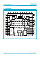
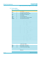
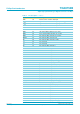
7.2 Pin description
Table 3: Pin description
Symbol Pin Description
n.c. 1 not connected
DEC2 2 main regulator decoupling input 2
V
ref
3 gain stabilizer voltage reference input
DEC1 4 main regulator decoupling input 1
n.c. 5 not connected
RAGC 6 red channel AGC output
RBOT 7 red channel ladder decoupling input (BOT)
RGAINC 8 red channel gain capacitor input
RCLP 9 red channel gain clamp capacitor input
RDEC 10 red channel gain regulator decoupling input
V
CCA(R)
11 red channel gain analog power supply
RIN 12 red channel gain analog input
AGND
R
13 red channel gain analog ground
GAGC 14 green channel AGC output
GBOT 15 green channel ladder decoupling input (BOT)
GGAINC 16 green channel gain capacitor input
GCLP 17 green channel gain clamp capacitor input
GDEC 18 green channel gain regulator decoupling input
V
CCA(G)
19 green channel gain analog power supply
GIN 20 green channel gain analog input
AGND
G
21 green channel gain analog ground
BAGC 22 blue channel AGC output
BBOT 23 blue channel ladder decoupling input (BOT)
BGAINC 24 blue channel gain capacitor input
BCLP 25 blue channel gain clamp capacitor input
BDEC 26 blue channel gain regulator decoupling input
V
CCA(B)
27 blue channel gain analog power supply
BIN 28 blue channel gain analog input
AGND
B
29 blue channel gain analog ground
n.c. 30 not connected
n.c. 31 not connected
I
2
C/3W 32 selection input between I
2
C-bus (active HIGH) and 3-wire
serial bus (active LOW)
ADD1 33 I
2
C-bus address control input 1
ADD2 34 I
2
C-bus address control input 2
TCK 35 scan test mode input (active HIGH)
TDO 36 scan test output
DIS 37 I
2
C-bus and 3-wire serial bus disable control input (disable at
HIGH level)
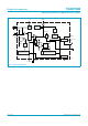
SEN 38 select enable for 3-wire serial bus input (see Figure 10)