
Data Sheet


QSB363 / QSB363GR / QSB363YR / QSB363ZR — Subminiature Plastic Silicon Infrared Phototransistor
© 2005 Fairchild Semiconductor Corporation www.fairchildsemi.com
QSB363 / QSB363GR / QSB363YR / QSB363ZR Rev. 1.1.0 2
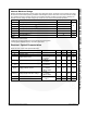
Absolute Maximum Ratings
Stresses exceeding the absolute maximum ratings may damage the device. The device may not function or be opera-
ble above the recommended operating conditions and stressing the parts to these levels is not recommended. In addi-
tion, extended exposure to stresses above the recommended operating conditions may affect device reliability. The
absolute maximum ratings are stress ratings only.
Values are at T
A
= 25°C unless otherwise specified.
Notes:
1. RMA flux is recommended.
2. Methanol or isopropyl alcohols are recommended as cleaning agents.
3. Derate power dissipation linearly 1.08 mW/°C above 25°C.
Electrical / Optical Characteristics
Values are at T
A
= 25°C unless specified otherwise.
Symbol Parameter Min. Unit
T
OPR
Operating Temperature -40 to +85
°C
T
STG
Storage Temperature -40 to +85
T
SOL-I
Soldering Temperature (Iron)
(1,2)
260
T
SOL-F
Soldering Temperature (Flow)
(1,2)
260
V
CEO
Collector Emitter Voltage 30
V
ECO
Emitter Collector Voltage 5 V
P
C
Power Dissipation
(3)
75 mW
Symbol Parameter Test Conditions Min. Typ. Max. Units
λ
P
Peak Sensitivity Wavelength
940 nm
Θ Reception Angle ±12
o
I
CEO
Collector Dark Current
V
CE
= 20 V,
E
e
= 0 mW/cm
2
100
nA
BV
CEO
Collector-Emitter Breakdown Voltage
I
C
= 100 μA,
E
e
= 0 mW/cm
2
30 V
BV
ECO
Emitter-Collector Breakdown Voltage
I
E
= 100 μA,
E
e
= 0 mW/cm
2
5V
I
C(ON)
On-State Collector Current
V
CE
= 5 V,
E
e
= 1 mW/cm
2
,
λ = 940 nm GaAs
1.0 1.5 mA
V
CE(SAT)
Collector-Emitter Saturation Voltage
I
C
= 2 mA,
E
e
= 1 mW/cm
2
,
λ = 940 nm GaAs
0.4
V
t
r
Rise Time
V
CE
= 5 V, I
C
= 1 mA,
R
L
= 1000 Ω
15 μs
t
f
Fall Time 15 μs