
Datasheet


ASQ1
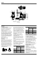
2. Right side pin type (Solder terminal only)
Simulated leaf lever
Note: When switching at high speed or under shock, lever endurance may drop. Therefore,
please be sure to conduct an endurance evaluation under actual switching conditions.
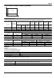
2.8
FP 14.4 MAX.
FP 18.6 MAX.
1.9dia.
15.0
R2.0
TTP (8.7)
OP (NO) 12.0±0.5
RP (NO) 12.4±0.5
OP (NC) 12.5±0.5
RP (NC) 12.9±0.5
TTP (12.9)
OP (NO) 16.2±0.5
RP (NO) 16.6±0.5
OP (NC) 16.7±0.5
RP (NC) 17.1±0.5
(18
°)
3.3
R1.3
0.5
C0.3
1.2
8.4±0.2
2.0
5.4±0.15
5.4
0.4
4.53±0.15
2.7
4.53±0.15
4.1
13.3±0.15
3.0
+0
–0.1
dia.
1.5
0.4
8.3±0.1
3.0
+0.3
–0.2
4.2
5.9
3.7
5.1
3.0
+0.1
–0
1.2
3.2±0.1
Operating Force (max. O.F.) 1.5N
Free
Position
(max. F.P.)
From mounting boss
and hole center line
14.4mm
From standoff 18.6mm
Operating
Position on
NC side
O.P. (N.C.)
From mounting boss
and hole center line
12.5±0.5mm
From standoff 16.7±0.5mm
Operating
Position on
NO side
O.P. (N.O.)
From mounting boss
and hole center line
12.0±0.5mm
From standoff 16.2±0.5mm
Release
Position on
NC side
R.P. (N.C.)
From mounting boss
and hole center line
12.9±0.5mm
From standoff 17.1±0.5mm
Release
Position on
NO side
R.P. (N.O.)
From mounting boss
and hole center line
12.4±0.5mm
From standoff 16.6±0.5mm
Over travel on N.C. side
(min. O.T. (N.C.))
3.3mm
Over travel on N.O. side
(min. O.T. (N.O.))
2.8mm
mm General tolerance: ±0.25
Mounting hole: 3 mm without boss type PC board terminal
PC board pattern
0.9
5.08±0.155.08±0.15
3.0
+0.3
−0.2
C0.2
5.08±0.15.08±0.1
1.0
+0.1
−0
dia.
8.3±0.1
C 0.2
8.3
2.6±0.05
2.2±0.05 dia.
2.6±0.05
5.0
1.9 dia.
0.4
1.5
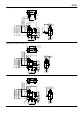
FP 13.4 MAX.
RP (NC) 13.0±0.3
OP (NC) 12.9±0.3
RP (NO) 12.7±0.3
OP (NO) 12.6±0.3
TTP (10.1)
FP 9.2 MAX.
RP (NC) 8.8±0.3
OP (NC) 8.7±0.3
RP (NO) 8.5±0.3
OP (NO) 8.4±0.3
TTP (5.9)
5.1
5.94.2
3.7
−0.2
+0.3
3.0
1.2
2.0
5.4±0.15
5.4
0.4
4.53±0.15
2.7
4.53±0.15
4.1
13.3±0.15
All Rights Reserved © COPYRIGHT Matsushita Electric Works, Ltd.