ORDER NO. DSC0603011CE B26 Digital Camera DMC-TZ1PP DMC-TZ1PL DMC-TZ1EB DMC-TZ1EE DMC-TZ1EF DMC-TZ1EG DMC-TZ1EGM DMC-TZ1GC DMC-TZ1GK DMC-TZ1GN DMC-TZ1GT DMC-TZ1SG Vol. 1 Colour (S)...........Silver Type (K)...........Black Type (A)...........Blue Type (except PL/GN/GT) © 2006 Matsushita Electric Industrial Co., Ltd. All rights reserved. Unauthorized copying and distribution is a violation of law.
TABLE OF CONTENTS PAGE 1 Safety Precaution -------------------------------------------------3 1.1. General Guidelines ----------------------------------------3 1.2. Leakage Current Cold Check ---------------------------3 1.3. Leakage Current Hot Check (See Figure 1.)--------3 1.4. How to Discharge the Capacitor on Power/Top PCB------------------------------------------------------------4 2 Warning --------------------------------------------------------------5 2.1.
1 Safety Precaution 1.1. General Guidelines 1.3. 1. IMPORTANT SAFETY NOTICE There are special components used in this equipment which are important for safety. These parts are marked by 2. 3. 4. 5. 1. Plug the AC cord directly into the AC outlet. Do not use an isolation transformer for this check. 2. Connect a 1.5 kΩ, 10 W resistor, in parallel with a 0.15 μF capacitor, between each exposed metallic part on the set and a good earth ground, as shown in Figure 1. 3.
1.4. How to Discharge the Capacitor on Power/Top PCB CAUTION: 1. Be sure to discharge the capacitor on POWER/TOP PCB. 2. Be careful of the high voltage circuit on POWER/TOP PCB when servicing. [Discharging Procedure] 1. Refer to the disassemble procedure and Remove the necessary parts/unit. 2. Put the insulation tube onto the lead part of Resistor (ERG5SJ102:1kΩ /5W). (an equivalent type of resistor may be used.) 3. Put the resistor between both terminals of capacitor on POWER/TOP PCB for approx.
2 Warning 2.1. Prevention of Electro Static Discharge (ESD) to Electrostatically Sensitive (ES) Devices Some semiconductor (solid state) devices can be damaged easily by static electricity. Such components commonly are called Electrostatically Sensitive (ES) Devices. The following techniques should be used to help reduce the incidence of component damage caused by electro static discharge (ESD). 1.
2.3. 2.3.1. Caution for AC Cord (For EB/GC/SG) 2.3.2.1. Information for Your Safety Blue Brown IMPORTANT Your attention is drawn to the fact that recording of prerecorded tapes or discs or other published or broadcast material may infringe copyright laws. WARNING To reduce the risk of fire or shock hazard, do not expose this equipment to rain or moisture. CAUTION To reduce the risk of fire or shock hazard and annoying interference, use the recommended accessories only.
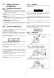
2.4. 2.4.1. How to Replace the Lithium Battery Replacement Procedure 1. Remove the POWER/TOP PCB. (Refer to Disassembly Procedures.) 2. Remove the Lithium battery (Ref. No. “Z9901” at component side of POWER/TOP PCB) and then replace it into new one. NOTE: This Lithium battery is a critical component. (Type No.: ML-421S/ZT Manufactured by Matsushita Battery Industrial Co.,Ltd.) It must never be subjected to excessive heat or discharge.
NOTE: Above caution is applicable for a battery pack which is for DMC-TZ1 series, as well.
3 Service Navigation 3.1. Introduction This service manual contains technical information, which allow service personnel’s to understand and service this model. Please place orders using the parts list and not the drawing reference numbers. If the circuit is changed or modified, the information will be followed by service manual to be controlled with original service manual. 3.2.
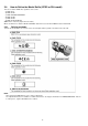
3.4. How to Define the Model Suffix (NTSC or PAL model) There are six kinds of DMC-TZ1, regardless of the colours. • a) DMC-TZ1S • b) DMC-TZ1PP • c) DMC-TZ1EB/EF/EG/EGM/GN • d) DMC-TZ1EE • e) DMC-TZ1GT • g) DMC-TZ1PL/GC/GK/SG (DMC-TZ1S is exclusively Japan domestic model.) What is the difference is that the “INITIAL SETTINGS” data which is stored in Flash ROM mounted on Main PCB. 3.4.1.
3.4.2. INITIAL SETTINGS: When you replace the Main PCB be sure to perform the initial settings after achieving the Adjustment, by ordering the following procedure in accordance with model suffix. • Step 1. The temporary cancellation of factory setting: Set the mode dial to “[ Normal picture mode ] (Red camera mark)”. While keep pressing [ Optical Image Stabilizer ] and “[ UP ] of Cross key” simultaneously, turn the Power on. • Step 2.
4 Specifications 12
5 Location of Controls and Components 13
6 Service Mode 6.1. Error Code Memory Function 1. General description This unit is equipped with history of error code memory function, and can be memorized 32 error codes in sequence from the latest. When the error is occurred more than 32, the oldest error is overwritten in sequence.
• 4. How to read the error code: One error code is displayed for 8 bit, the contents of error codes is indicated the table as shown below. Attribute LENS Main item Lens drive Sub item OIS C.B./Zoom Zoom Focus Lens Error code Contents (Upper) High 4 bits Low 4 bits Check point (Lower) 1800 1000 PSD (X) error. Hall element (X axis) position detect error in OIS unit. OIS Unit 2000 PSD (Y) error. Hall element (Y axis) position detect error in OIS unit. OIS Unit 3000 GYRO (X) error.
Attribute Main item LENS Adj.History HARD VENUS A/D FLASH ROM (EEPROM Area) SYSTEM SOFT CPU Card CPU, ASIC hard Operation Zoom Sub item Error code Contents (Upper) High 4 bits Low 4 bits Check point (Lower) OIS 1900 2000 OIS adj. Yaw direction amplitude error (small) OIS Unit, LENS flex breaks. 3000 OIS adj. Pitch direction amplitude error (small) OIS Unit, LENS flex breaks. 4000 OIS adj. Yaw direction amplitude error (large) OIS Unit, LENS flex breaks. 5000 OIS adj.
6.2. Confirmation of Firmware Version The Firmware version can be confirmed by ordering the following steps:. • Step 1. The temporary cancellation of factory setting: Set the mode dial to “[ Normal picture mode ] (Red camera mark)”. Insert the SD memory card which has a few photo data. While keep pressing [ Optical Image Stabilizer ] and “[ UP ] of Cross key” simultaneously, then turn the power on. • Step 2.
7 Service Fixture & Tools 7.1. Service Fixture and Tools The following Service Fixture and tools are used for checking and servicing this unit.
7.2. When Replacing the Main PCB After replacing the MAIN PCB, be sure to achieve adjustment. The adjustment instruction is available at “software download” on the “Support Information from NWBG/VDBG-PAVC” web-site in “TSN system”, together with Maintenance software. 7.3. Service Position This Service Position is used for checking and replacing parts. Use the following Extension cables for servicing. Table S1 Extension Cable List No. 1 2 3 4 5 6 Parts No.
8 Disassembly and Assembly Instructions 8.1. Disassembly Flow Chart 8.2.
8.3. Disassembly Procedure No. Item 1 Rear Case Unit Fig Fig. D1 2 3 LCD Unit Front Case Unit Fig. D2 Fig. D3 Fig. D4 4 Main P.C.B. Fig. D5 5 Top Operation Unit Fig. D6 Fig. D7 6 Jack P.C.B. Fig. D8 7 Power/Top P.C.B. Fig. D9 Fig. D10 8 Lens Unit Fig. D11 Fig. D12 9 SD/AFE P.C.B. Fig. D13 Fig. D14 10 Battery Door Unit Battery Case Unit Fig. D15 11 Battery Case Fig. D16 8.3.1.
8.3.2. Removal of the LCD Unit Fig. D2 Fig.
8.3.3. Removal of the Front Case Unit 8.3.4. Removal of the Main P.C.B. Fig. D5 Fig. D4 Fig.
8.3.5. Removal of the Top Operation Unit 8.3.7. Removal of the Power/Top P.C.B. Fig. D7 8.3.6. Removal of the Jack P.C.B. Fig. D9 Fig.
Fig. D11 8.3.8. Removal of the Lens Unit Fig. D10 Fig.
8.3.10. Removal of the Battery Door Unit and Battery Case Unit Fig. D13 8.3.9. Removal of the SD/AFE P.C.B. Fig. D15 Fig.
8.3.11. 8.4. Removal of the Battery Case Disassembly Procedure for the Lens NOTE: When Disassembling and Assembling for the Lens 1. To minimize the possibility of the CCD being dirt, perform disassemble and/or assemble under the condition of the CCD is being mounted. Disassembling procedures for the CCD unit, refer to item 8.6. 2. Take care that the dust and dirt are not entered into the lens. In case of the dust is putted on the lens, blow off them by airbrush. 3. Do not touch the surface of lens. 4.
8.4.1. Removal of the 1st Lens Frame/ Drive Frame/Fixed Frame Unit 8.4.2. 1. Unscrew the 2 screws (A). 2. Depress the zoom motor unit to relese the locking tabs (2 pcs), and then remove to the indicated by arrow. 3. Unscrew the 2 screws (B). 4. Unscrew the 1 screw (C). 5. Remove the 1st lens frame/drive frame/fixed frame unit. Removal of the 1st Lens Frame Unit and Drive Frame Unit • Turn the drive gear to the indicated by arrow fully, and then remove the 1st lens frame unit and drive frame unit.
8.5. Assembly Procedure for the Lens 8.5.1. Phase alignment of the Drive Frame Unit and Fixed Frame Unit 8.5.2. Phase alignment of the 1st Lens Frame Unit and Drive Frame/Fixed Frame Unit 8.5.3.
8.6. Removal of the CCD Unit To prevent the CCD unit from catching the dust and dirt, do not remove the CCD unit except for replacing.
9 Measurements and Adjustments 9.1. Matrix Chart for Replaced Part and Necessary Adjustment The relation between Replaced part and Necessary Adjustment is shown in the following table. When concerned part is replaced, be sure to achieve the necessary adjustment(s). As for Adjustment condition/procedure, consult the “Adjustment Manual” which is available in Adjustment software.
10 Maintenace 10.1. Cleaning Lens and LCD Panel Do not touch the surface of lens and LCD Panel with your hand. When cleaning the lens, use air-Blower to blow off the dust. When cleaning the LCD Panel, dampen the lens cleaning paper with lens cleaner, and the gently wipe the their surface. Note: The Lens Cleaning KIT ; VFK1900BK (Only supplied as 10 set/Box) is available as Service Aid.
DSC0603011CE Service Manual S1. About Indication of The Schematic Diagram S1.1. Important Safety Notice COMPONENTS IDENTIFIED WITH THE MARK HAVE THE SPECIAL CHARACTERISTICS FOR SAFETY. WHEN REPLACING ANY OF THESE COMPONENTS USE ONLY THE SAME TYPE. Diagrams and Replacement Parts List 1.Although reference number of the parts is indicated on the P.C.B. drawing and/or schematic diagrams, it is NOT mounted on the P.C.B. when it is displayed with "$" mark. Digital Camera 3.
S2. Voltage Chart Note) Indicated voltage values are the standard values for the unit measured by the DC electronic circuit tester (high-impedance) with the chassis taken as standard. Therefore, there may exist some errors in the voltage values, depending on the internal impedance of the DC circuit tester. S2.1. Power Top P.C.B. REF No. PIN No. REC REF No. PIN No. REC IC1004 1 2.8 Q1003 4 3.6 IC1004 2 0 Q1003 5 3.6 IC1004 3 1.2 Q1003 6 3.5 IC1004 4 8.
S3. Block Diagram S3.1. Overall Block Diagram (35mm ~ 350mm) IC3101 CCD 1/2.5" 6.
S3.2. System Control Block Diagram IC6001 (VENUS3/MICRO PROCESSOR) IC6003 POWER SW ON 308 BA1 24 75 SDBA1 Bank Adr. Bank Adr. BA0 23 76 SDBA0 DQ15 88 29 SDD15 DATA DQ0 POWER SW ON(H) SHUTTER HALF SHUT HALF 177 SHUTTER FULL SHUT FULL 174 RL9113 RL9114 DATA SELF LED ON 169 LED IN 0 44 36 8 35 9 A11 22 SHUTTER 0 SHUTTER 1 FP9001 38 FP9001 40 FP9001 42 FP9001 14-17 POWER / TOP P.C.B.
S3.3.
S3.4. Sensor Block Diagram CL3012 CL3013 To IC8001-2 (FLASH TRG) To IC6001-199 (CCDVD) IC3101 To IC6001-200 (CCDHD) IC3004 (CCD IMAGE SENSOR) (CDS/AGC/AD/TG) 34 FLASH VO 16 FP6501 30 3 2 26 CCD IN 36 VD 37 HD AGC (PGA) CDS D0 39 A/D (12bit) 12bit D11 50 1 CL3011 Q3101 53 VSUB 4 5 To IC6001-197 (FCK) (24.
S3.5. Lens Drive Block Diagram IC6001 QR7004 FP9004 CO BARREL & FOCUS ENC 37 QR7002 ZENC LUT MCK48I 4 6 ZENC1 29 MCK48O 6 246 ZENC LUT 241 ZENC LEDCNT ZENC1 LED K 28 39 5 4 X6001 (48MHz) ZENC2 32 MR SENSOR 242 ZHP LEDCNT ZHP LED K ZENC2 LED K 31 ZOOM ENC (VENUS3) 4 GND MRB 2 MRA 4 1 2 MB MA REFO 24 25 26 31 GND 2 253 ZENC2 LEDCNT CR NET CCD 1 3 3 29 30 18 20 247 ZENC1 IC6006 19 248 ZENC2 AIN PRISM GRASS OPTICAL FILTER BIN A3.1V REFI VM1 FP9004 M AF3.
S3.6. Power Block Diagram CL1003 JK2002 F2001 UNREG+ 1 UNREG CL1010 CL1004 5V CL1008 AF3.4V CL1007 CL1002 BATTERY TERMINAL F1002 MAIN A3.1V A3.1V Q1003 F1001 (MOS-FET: Pch) QR1001 D G Q1001 (MOS-FET: Nch) S D G 4 Q1002 6 IC1001 6 5 2 1 32 SCP VBAT HX1 SCP 3 PVCC S LX1 LX1 CL9012 CH1 (N/Pch) FP9901 FP9001 26 27 UDSEL1 INV1 PGND12 STEP UP/ DOWN SEL. QR1006 QR1002 PVCC HX2 CH2 (N/Pch) INV2 LX2 IC9101 POWER / TOP P.C.B.
20 19 18 17 16 15 14 13 12 11 NC NC VIDEO GND SELF LED A SELF LED K UNREG GND UNREG GND UNREG GND UNREG GND UNREG GND S-9 2 MRB 4 MRA 6 FM P 8 X VH+ 10 X VH12 Y DR+ 14 X VO+ 16 X DR+ 18 Y VO20 SHUT2 22 SHUT1 24 IRIS1 26 IRIS2 28 TME1 LED K 30 TME1 TME2 VCC 32 TME2 34 DCM+ 36 DCM38 CHP VCC 1 USB(+) 2 USB(-) 3 USB GND 4 VIDEO OUT 5 USB CABLE IN 6 CABLE DET 7 LINE OUT 8 UNREG+ 9 UNREG+ 10 UNREG+ NC D GND MR VCC FM N X VOY VHY DRX DRY VH+ Y VO+ SHU2 SHUT1 IRIS1 IRIS2 TME1 TME2LED K DCM+ DCMCHP LED K CHP PP20
S4.2. Power (P) Schematic Diagram 1/4 DMC-TZ1 Power Section (Power Top P.C.B. (1/4)) Schematic Diagram (P) N CAUTION: FOR CONTINUED PROTECTION AGAINST FIRE HAZARD, REPLACE ONLY WITH THE SAME TYPE 1.5A 32V FUSE. ATTENTION: POUR UNE PROTECTION CONTINUE LES RISQUES 1.5A 32V D' INCENDIE N' UTILISERQUE DES FUSIBLE DE MÉME TYPE 1.5A 32V. M %. 6% %. %. 6% 704') 6% $#6 6% $#6̂ & %. 4. ( L 1.
2/4 4. 6% # 4. 6% 4. % ( , , # 6% %. 4. 4 4 #( 4 8 6% # %. = ? 6% # 4 8 6% # 4 8 6% & 4 8 6% % W= ? 8QWV +% % %$#$% 8 0R % = ? )0& 8EPV )0& 8KP % W= ? 8QWV +% % %$#$% 8 0R )0& 4 -=&? )0& 8EPV 4 - 4 -=&? 8KP % 6% 56 %. . ) % 4 <# % '%, ($ , - 704') % = ? %.
6% 1 2 3 4 ) 5 & 5 S-12 3 $ %(*% C 4 4 6 7 4 - 3 $ &($% % ( , % 4 - % D 4 4 8 ) A 3/4 5 9 -=&? 34 704 , . 10 % '%, 8$ , - ( * # # 56$ +08 +08 = ?+08 + 010 84'( )0& 5%2 8%% 84')# 46 +08 +08 = ?7&5'. = ?+08 % +08 % 4 7&5'. % '%, 8$ , - 4 H 8$#6 G F E 6% %. .
4 % = ? & 4 8 6% & 4 8 6% 4 -=&? +% % &$#(' 8176 %' 8+0 .: %. . ) % 4 <# = ? 4 4 = ? 3 $ %(*% % % '%, ($ , - 855 855 ( , , # 4 -=&? '%, 8$ , - 4 & ) 5 %. 4 = ? 6% % +% % %$%)% 02 8QWV 8EQPV 8KP 4 )0& )0& +08 010 56$ +08 % W= ? % %. %%& 8 & /# & .
S4.3. Audio (A) Schematic Diagram F 4 %. G 34 704 , . 6% $+#5176 #$+#5 5�# 5%.- 4 6% % = ? ( , # # # 4 8 2 6% 6% .+0'176 &855 6% % W= ? % 4 %. %. 4 .0( '84176 C 4 %. 6#7 % 52+0 5'0 $''2+0 52)0& % 4 %.
S4.4. Flash (ST) Schematic Diagram G F 1.25A 32V 6. 6. 64)= PF? 6. .#/2= ? .#/2=̂? 1.25A 32V & $ *%/2 6 ) ( # 4 /=&? = ? % ( - , # = ? ) ' 4 /=&? = ? %. & % ( - ' = ? % 5 ) - % ( # ( 8 Ǵ( 64)= UV? 5 4 %. 4 /= ? ( , # # = ? 5 704') 5 3 $ ,$.2 D ( - * % 64)=%1/? %.
S4.5. Top Connection (TC) Schematic Diagram %. %. % 4 #4'% 8 4 2.#; 8 4 5;/2.' 8 4 - 5%'0' 8 4 - 5%'0' 8 % F /#%41 $#6 8# 4 2 =& '& 4 # ? 8 $#6̂ $#6̂ /18+' 8 2 ,- - << %.
S4.6. Jack Schematic Diagram G F 4 - 4 - . , ,#& E #8 75$ .$ , ,#% ,- - ($ ' /+657/+ 22 - -# $# 75$ 0% 75$ ̂ 0% 704') 704') 704') D 75$ 75$̂ .$ , ,%% .$ , ,$% .$ , ,%% (4#/'a)0& 4 4 = ? ( '4$5' 4 7 6. 4 &% ,- - ;< *15+&'0 1.
S4.7. CCD Flex Schematic Diagram G F (6 8 $ 8 # 8 . 8 4 8 8 5 8 8 # 8 = ? ( , # % % 4 3 72 . 8 # 8 $57$ 57$ 8 . 4 *. * * 8 4 8 . 8.
S4.8.
S5. Print Circuit Board S5.1. Power Top P.C.B. G 4 4 % 4 4 % 4 4 4 4 4 % 4 4 4 4 4 % %+ % .6 5 4 '6 3 43 5 #8 #8 5 4. 4 4 & 4 3 % 4 4 4 .6 6 6 4 4 6.
S5.2. Jack P.C.B. 22 G & 4 4 $. F 4 -, . -, E (Component Side) D % C 4 4 %. %. ( B 4 .$ .$ 6. .$ .$ (Foil Side) A DMC-TZ1 Jack P.CB.
S5.3. CCD Flex P.C.B. G F E D (Component Side) (6 +% C % % B 4 4 6* 4 % 3 4 4 4 (Foil Side) A DMC-TZ1 CCD Flex P.C.B.
S5.4. Lens Flex P.C.B. B LINEAR ACTUATOR E B1 A4 A3 A2 A1 B2 C1 C2 C3 C6 C5 C4 C11 C10C12 C9 Pin 39 D2 D SHUTTER MOTOR D1 E1 C OIS UNIT C7 C8 D Pin 1 A MR SENSOR E IRIS MOTOR E2 C F ZOOM ENCODER 1 F3 F2 I2 B F1 I3 G2 I1 G3 I ZOOM DETECTION G1 G ZOOM ENCODER 2 H2 A H1 H ZOOM MOTOR DMC-TZ1 LENS FLEX P.C.B.
S-24
S6. Replacement Parts List Note: 1.* Be sure to make your orders of replacement parts according to this list. 2. IMPORTANT SAFETY NOTICE Components identified with the mark have the special characteristics for safety. When replacing any of these components, use only the same type. 3. Unless otherwise specified, All resistors are in OHMS, K=1,000 OHMS. All capacitors are in MICRO-FARADS (uf), P=uuF. 4. The marking (RTL) indicates the retention time is limited for this item.
DMC-TZ1PP/PL/EG/EGM/EF/EB/EE/GC/SG/GT/GK/GN/GD vol.1 Ref.No. Part No. Part Name & Description Pcs VEP56033A VEP51005A VEP53030A VEP59026A VXW0797 ------ P.C.B. LIST -----MAIN P.C.B. POWER/TOP P.C.B. SD/AFE P.C.B. JACK P.C.B. CAMERA LENS UNIT F2A2F8500002 VSQ1235 K4ZZ03000324 L0FZBA000004 ML-421S/ZT --- INDIVIDUAL PARTS --E.CAPACITOR EARTH SPRING BATTERY CATCHER MICROPHONE BATTERY VEP51005A --- ELEC. COMPONENTS --POWER/TOP P.C.B.
DMC-TZ1PP/PL/EG/EGM/EF/EB/EE/GC/SG/GT/GK/GN/GD vol.1 Ref.No. Part No.
DMC-TZ1PP/PL/EG/EGM/EF/EB/EE/GC/SG/GT/GK/GN/GD vol.1 Ref.No. Part No. Part Name & Description Pcs VXW0802 -- CASING/LENS SECTION -REAR CASE UNIT REAR CASE UNIT REAR CASE UNIT STRAP ORNAMENT STRAP ORNAMENT FRONT CASE UNIT FRONT CASE UNIT FRONT CASE UNIT SD/AFE P.C.B. MAIN P.C.B. JACK P.C.B. BUZZER BATTERY FLASH UNIT POWER/TOP P.C.B.
DMC-TZ1PP/PL/EG/EGM/EF/EB/EE/GC/SG/GT/GK/GN/GD vol.1 Ref.No. Part No. Part Name & Description Pcs Remarks Ref.No.
S7. Exploded View S7.1.
S7.2.