
- Pep Smart I/O User's Manual
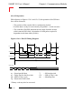
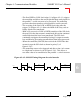

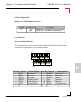
Table Of Contents
- Preface.pdf
- Introduction.pdf
- Table of Contents
- General Information
- Weights & Measures
- 1.1 Product Overview
- 1.2 Ordering Information
- 1.3 Product Information
- 1.4 Installation
- 1.4.1 Overview
- 1.4.2 SMART I/O Module Installation
- 1.4.3 RJ45 Telephone Connector Installation
- 1.4.4 Screw Terminal Block Installation
- 1.4.5 Battery Installation
- 1.5 ISaGRAF-Installation
- 1.5.1 Before Installing
- 1.5.2 Installation of the ISaGRAF for Windows Workbench
- 1.5.3 Installation of PEP Library Functions
- 1.5.4 Demo Application
- Table of Contents
- SM-BASE.pdf
- Table of Contents
- 2. SMART-BASE
- 2.1 Specifications
- 2.2 Board Overview
- 2.3 Functional Description
- 2.4 Configuration
- 2.4.1 Jumper J1: Boot Selection (Pin Connector)
- 2.4.2 Jumper J6: LED Function (Pin Connector)
- 2.5 Pinouts
- 2.5.1 SMART Module Piggyback Connectors
- 2.5.2 Screw Terminal Pinouts
- 2.5.3 Timer I/O Screw Terminal (SCR1)
- 2.5.4 Supply Screw Terminals (SCR2)
- 2.5.5 RS232 Telephone Connector (BU1)
- 2.5.6 RS485 D-Sub Connector for Half-Duplex Operation (Profibus)
- 2.5.7 SPI Connector (ST7)
- 2.6 ‘C’ Programming
- 2.6.1 SMART-BASE Library
- 2.6.2 SMTselIn
- 2.6.3 SMTsettout
- 2.6.4 SMTpre
- 2.6.5 SMTstasto
- 2.6.6 SMTrd
- 2.6.7 SMTtin
- 2.6.8 SMTstat
- 2.6.9 SMTout
- 2.6.10 SMLed
- 2.6.11 SMwdon
- 2.6.12 SMwdtrig
- 2.6.13 SMwdoff
- 2.7 ISaGRAF Programming
- 2.7.1 The ISaGRAF Board Parameters
- 2.7.2 The ISaGRAF Operate Calls
- 2.8 Flash Utility
- Table of Contents
- SM-EXT.pdf
- Digital.pdf
- Table of Contents
- 4. Digital Modules
- 4.1 SM-DIN1
- 4.1.1 Introduction
- 4.1.2 Specifications
- 4.1.3 Front Panel Layout
- 4.1.4 Board Overview
- 4.1.5 Functional Description
- 4.1.6 Configuration
- 4.1.7 Pinouts
- 4.1.8 ‘C’ Programming
- 4.1.8.1 SM-DIN1 Library
- 4.1.8.2 SMDIN1Init
- 4.1.8.3 SMDIN1DeInit
- 4.1.8.4 SMDIN1Get
- 4.1.9 ISaGRAF Programming
- 4.1.9.1 The ISaGRAF Board Parameters
- 4.1.9.2 The ISaGRAF Operate Calls
- 4.2 SM-DOUT1
- 4.2.1 Introduction
- 4.2.2 Specifications
- 4.2.3 Front Panel Layout
- 4.2.4 Board Overview
- 4.2.5 Functional Description
- 4.2.6 Configuration
- 4.2.7 Pinouts
- 4.2.8 ‘C’ Programming
- 4.2.8.1 SM-DOUT1 Library
- 4.2.8.2 SMDOUT1Init
- 4.2.8.3 SMDOUT1DeInit
- 4.2.8.4 SMDOUT1Get
- 4.2.8.5 SMDOUT1Set
- 4.2.9 ISaGRAF Programming
- 4.2.9.1 The ISaGRAF Board Parameters
- 4.2.9.2 The ISaGRAF Operate Calls
- 4.3 SM-REL1
- 4.3.1 Introduction
- 4.3.2 Specifications
- 4.3.3 Front Panel Layout
- 4.3.4 Board Overview
- 4.3.5 Functional Description
- 4.3.6 Configuration
- 4.3.7 Pinouts
- 4.3.8 ‘C’ Programming
- 4.3.8.1 SM-REL1 Library
- 4.3.8.2 SMREL1Init
- 4.3.8.3 SMREL1DeInit
- 4.3.8.4 SMREL1Reset
- 4.3.8.5 SMREL1GetRly
- 4.3.8.6 SMREL1SetRly
- 4.3.8.7 SMREL1GetLed
- 4.3.8.8 SMREL1SetLed
- 4.3.8.9 SMREL1GetExtVcc
- 4.3.9 ISaGRAF Programming
- 4.3.9.1 The ISaGRAF Board Parameters
- 4.3.9.2 The ISaGRAF Operate Calls
- Table of Contents
- Analog.pdf
- Table of Contents
- 5. Analog Modules
- 5.1 SM-DAD1
- 5.1.1 Introduction
- 5.1.2 Specifications
- 5.1.3 Front Panel Layout
- 5.1.4 Board Overview
- 5.1.5 Functional Description
- 5.1.5.1 Input Circuitry
- 5.1.5.2 Output Circuitry
- 5.1.6 Configuration
- 5.1.7 Pinouts
- 5.1.8 ‘C’ Programming
- 5.1.8.1 SM-DAD1 Library
- 5.1.8.2 SMDAD1Init
- 5.1.8.3 SMDAD1DeInit
- 5.1.8.4 SMDAD1GetVRaw
- 5.1.8.5 SMDAD1GetV
- 5.1.8.6 SMDAD1PutVRaw
- 5.1.8.7 SMDAD1PutV
- 5.1.8.8 SMDAD1SetLed
- 5.1.8.9 SMDAD1ClrLed
- 5.1.9 ISaGRAF Programming
- 5.1.9.1 The ISaGRAF Board Parameters
- 5.1.9.2 The ISaGRAF Operate Calls
- 5.2 SM-PT100
- 5.2.1 Introduction
- 5.2.2 Specifications
- 5.2.3 Front Panel Layout
- 5.2.4 Board Overview
- 5.2.5 Functional Description
- 5.2.6 Configuration
- 5.2.7 Pinouts
- 5.2.8 ‘C’ Programming
- 5.2.8.1 SM-PT100 Library
- 5.2.8.2 SMADCInit
- 5.2.8.3 SMADCCalibrate
- 5.2.8.4 SMADCSetCyclicCalib
- 5.2.8.5 SMADCSetSensorType
- 5.2.8.6 SMADCGetSensorType
- 5.2.8.7 SMADCSetPrecision
- 5.2.8.8 SMADCGetPrecision
- 5.2.8.9 SMADCSetMode
- 5.2.8.10 SMADCGetMode 5-47
- 5.2.8.11 SMADCSetSignal
- 5.2.8.12 SMADCSetGain
- 5.2.8.13 SMADCGetGain
- 5.2.8.14 SMADCEnableRead
- 5.2.8.15 SMADCEnableConversion
- 5.2.8.16 SMADCReadRaw
- 5.2.8.17 SMADCReadConverted
- 5.2.8.18 SMADCDeinit
- 5.2.9 ISaGRAF Programming
- 5.2.9.1 The ISaGRAF Board Parameters
- 5.2.9.2 The ISaGRAF Operate Calls
- 5.3 SM-THERM
- 5.3.1 Introduction
- 5.3.2 Specifications
- 5.3.3 Front Panel Layout
- 5.3.4 Board Overview
- 5.3.5 Functional Description
- 5.3.6 Configuration
- 5.3.7 Pinouts
- 5.3.8 ‘C’ Programming
- 5.3.8.1 SM-THERM Library
- 5.3.8.2 SMADCInit
- 5.3.8.3 SMADCCalibrate
- 5.3.8.4 SMADCSetCyclicCalib
- 5.3.8.5 SMADCSetSensorType
- 5.3.8.6 SMADCGetSensorType
- 5.3.8.7 SMADCSetPrecision
- 5.3.8.8 SMADCGetPrecision
- 5.3.8.9 SMADCSetMode 5-75
- 5.3.8.10 SMADCGetMode
- 5.3.8.11 SMADCSetSignal
- 5.3.8.12 SMADCSetGain
- 5.3.8.13 SMADCGetGain
- 5.3.8.14 SMADCEnableRead
- 5.3.8.15 SMADCEnableConversion
- 5.3.8.16 SMADCReadRaw
- 5.3.8.17 SMADCReadConverted
- 5.3.8.18 SMADCDeinit
- 5.3.9 ISaGRAF Programming
- 5.3.9.1 The ISaGRAF Board Parameters
- 5.3.9.2 The ISaGRAF Operate Calls
- 5.4 SM-ADC1
- 5.4.1 Introduction
- 5.4.2 Specifications
- 5.4.3 Front Panel Layout
- 5.4.4 Board Overview
- 5.4.5 Functional Description
- 5.4.5.1 Input Circuitry
- 5.4.6 Configuration
- 5.4.7 Pinouts
- 5.4.8 ‘C’ Programming
- 5.4.8.1 SM-ADC1 Library
- 5.4.8.2 SMADC1Init
- 5.4.8.3 SMADC1GetVRaw
- 5.4.8.4 SMADC1GetV
- 5.4.8.5 SMADC1SetLed
- 5.4.8.6 SMADC1ClrLed
- 5.4.8.7 SMADC1DeInit
- 5.4.9 ISaGRAF Programming
- 5.4.9.1 The ISaGRAF Board Parameters
- 5.4.9.2 The ISaGRAF Operate Calls
- 5.5 SM-DAC1
- 5.5.1 Introduction
- 5.5.2 Specifications
- 5.5.3 Front Panel Layout
- 5.5.4 Board Overview
- 5.5.5 Functional Description
- 5.5.5.1 Output Circuitry
- 5.5.6 Configuration
- 5.5.7 Pinouts
- 5.5.8 ‘C’ Programming
- 5.5.8.1 SM-DAC1 Library
- 5.5.8.2 SMDAC1Init
- 5.5.8.3 SMDAC1OpenLoop
- 5.5.8.4 SMADAC1Operate
- 5.5.8.5 SMDAC1StandBy
- 5.5.8.6 SMDAC1PutVRaw
- 5.5.8.7 SMDAC1PutV
- 5.5.8.8 SMDAC1SetLed
- 5.5.8.9 SMDAC1ClrLed
- 5.5.8.10 SMDAC1DeInit
- 5.5.9 ISaGRAF Programming
- 5.5.9.1 The ISaGRAF Board Parameters
- 5.5.9.2 The ISaGRAF Operate Calls
- Table of Contents
- Comms.pdf
- Table of Contents
- 6. Communications Modules
- 6.1 SM-RS232 6
- 6.1.1 Introduction
- 6.1.2 Specifications
- 6.1.3 Front Panel Layout
- 6.1.4 Board Overview
- 6.1.5 Functional Description
- 6.1.6 Configuration
- 6.1.7 Pinouts
- 6.1.8 ISaGRAF Programming
- 6.1.8.1 The ISaGRAF Board Parameters
- 6.1.8.2 The ISaGRAF Operate Calls
- 6.1.9 OS-9 Programming
- 6.2 SM-SSI
- 6.2.1 Introduction
- 6.2.2 Specifications
- 6.2.3 Front Panel Layout
- 6.2.4 Board Overview
- 6.2.5 Functional Description
- 6.2.6 SSI Operation
- 6.2.7 Register Description
- 6.2.7.1 Control Register
- 6.2.7.2 CTRL1 Register
- 6.2.7.3 CTRL2 Register
- 6.2.7.4 CTRL3 Register
- 6.2.7.5 Compare Register
- 6.2.7.6 Identification Register
- 6.2.7.7 Status Register
- 6.2.7.8 STAT1 Register
- 6.2.7.9 STAT2 Register
- 6.2.7.10 Data Register
- 6.2.8 MATCH Function
- 6.2.9 Tested Sensors
- 6.2.10 Configuration
- 6.2.11 Pinouts
- 6.2.12 ‘C’ Programming
- 6.2.12.1 SM-SSI Library
- 6.2.12.2 SMSSIInit
- 6.2.12.3 SMSSIDeInit
- 6.2.12.4 SMSSISetSetPoint
- 6.2.12.5 SMSSISetCtrlReg
- 6.2.12.6 SMSSIGetStatus
- 6.2.12.7 SMSSIGetData
- 6.2.13 ISaGRAF Programming
- 6.2.13.1 The ISaGRAF Board Parameters
- Table of Contents
SMART I/O User’s Manual
©1996 PEP Modular Computers GmbHOctober 01, 1996 Page 6 - 21
6
Chapter 6 Communications Modules
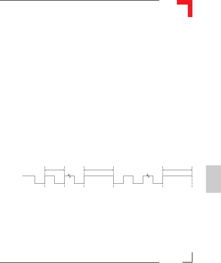
• The first HIGH to LOW clock edge (1) in figure 6.2.6.1, triggers
the monoflop and allows the current parallel data word present in
the parallel -> serial converter to be processed. The monoflop
prevents other data transfers to this parallel to serial converter.
• The crossing of the first LOW to HIGH clock edge after the
trigger (2) in figure 6.2.6.1 allows the MSB of the Gray code or
binary signal to be transferred.
• With every successive LOW to HIGH transition of the SSI clock,
the next bit in the data stream is transferred; this action continues
until all the data bits have been transferred. The SSI clock
continually retriggers the monoflop forcing it’s output to remain
low and thereby preventing unwanted data from being processed.
• When the controller (SM-SSI) has received the LSB of the data
stream it stops the SSI clock as shown in point (3) of
figure 6.2.6.1.
• The monoflop ceases to be triggered and after a time ‘tm’ returns
to a high state as shown in (4) of figure 6.2.6.1. This allows a
new data value to be transferred to the parallel -> serial converter.
T
Clock
Pause
Tp
Pause
Tp
Figure 6.2.6.2: SM-SSI Timing Diagram for serial transfer