IMPORTANT SAFETY NOTICE Proper service and repair is important to the safe, reliable operation of all Philips Consumer Electronics Company** Equipment. The service procedures recommended by Philips and described in this service manual are effective methods of performing service operations. Some of these service operations require the use of tools specially designed for the purpose. The special tools should be used when and as recommended.
FIRE AND SHOCK HAZARD 1. Be sure all components are positioned in such a way as to avoid the possibility of adjacent component shorts. This is especially important on those chassis which are transported to and from the service shop. 2. Never release a repaired unit unless all protective devices such as insulators, barriers, covers, strain reliefs, and other hardware have been installed in accordance with the original design. 3.
LEAKAGE CURRENT COLD CHECK 1. Unplug the ac line cord and connect a jumper between the two prongs of the plug. 2. Turn on the power switch. 3. Measure the resistance value between the jumpered ac plug and all exposed cabinet parts of the receiver, such as screw heads, antennas, and control shafts. When the exposed metallic part has a return path to the chassis, the reading should be between 1 megohm and 5.2 megohms.
TV SAFETY NOTES SAFETY CHECKS After the original service problem has been corrected, a complete safety check should be made. Be sure to check over the entire set, not just the areas where you have worked. Some previous servicer may have left an unsafe condition, which could be unknowingly passed on to your customer.
5. When troubleshooting and making test measurements in a receiver with a problem of excessive high voltage, reduce the line voltage by means of a Variac to bring the HV into acceptable limits while troubleshooting. Do not operate the chassis longer than necessary to locate the cause of the excessive HV. 6. New picture tubes are specifically designed to withstand higher operating voltages without creating undesirable X-radiation.
PREVENTION OF ELECTROSTATIC DISCHARGE (ESD) Some semiconductor solid state devices can be damaged easily by static electricity. Such components commonly are called Electrostatically Sensitive (ES) Devices, Examples of typical ES devices are integrated circuits and some field-effect transistors and semiconductor "chip" components. The following techniques should be used to help reduce the incidence of component damage caused by electrostatic discharge (ESD). 1.
PRACTICAL SERVICE PRECAUTIONS IT MAKES SENSE TO AVOID EXPOSURE TO ELECTRICAL SHOCK. While some sources are expected to have a possible dangerous impact, others of quite high potential are of limited current and are sometimes held in less regard. ALWAYS RESPECT VOLTAGES. While some may not be dangerous in themselves, they can cause unexpected reactions – reactions that are best avoided. Before reaching into the powered color TV set, it is best to test the high voltage insulation.
Technical Specifications, Connections and Chassis Overview Technical Specifications Reception Feature Data Tuning system : PLL Color systems (off-air) : NTSC M Sound systems : : BTSC DBX A/V connections : NTSC M, : NTSC Playback Channel selections : 181 channels, : Full-cable, UHF IF frequency : 45.
Miscellaneous Feature Data Set stroke numbers : /17 AC voltage : 120V (± 10%), AC frequency : 50 / 60Hz (± 5%) Ambient temperature : + 5 to + 45 deg. C. Standby Power consumption : 0.
S-Video Connector Kind Value Symbol 1 Gnd v 2 Gnd v 3 Y 1Vpp / 75 ohm j 4 C 0.3Vpp / 75 ohm j Connector Kind Value Symbol 1 Video 1Vpp / 75 ohm jq 2 Audio L (0.5Vrms / 10k) jq 3 Audio R (0.
Rear Connections Figure: Rear connections Monitor out Connector Kind Value Symbol 1 Video 1Vpp / 75 ohm kq 2 Audio L (0.5Vrms / 10k) kq 3 Audio R (0.5Vrms / 10k) kq Connector Kind Value Symbol 1 Y 0.7Vpp / 75 ohm jq 2 Pb 0.7Vpp / 75 ohm jq 3 Pr 0.
AV1 in Connector Kind Value Symbol 4 Video 1Vpp / 75 ohm jq 5 Audio L (0.5Vrms / 10k) jq 6 Audio R (0.5Vrms / 10k) jq Connector Kind Value Symbol 1 Video 1Vpp / 75 ohm jq 2 Audio L (0.5Vrms / 10k) jq 3 Audio R (0.5Vrms / 10k) jq Value Symbol 1 Gnd v 2 Gnd v AV2 in AV2 in (SVHS) Connector Kind 3 Y 1Vpp / 75 ohm j 4 C 0.
AV4 in (D-sub connector) Connector Kind Value Symbol 1 Pr/R 0.35 Vpp/0.7 Vpp / ohm jq 2 Y/G 0.7 Vpp/0.7 Vpp / 75 ohm jq 3 Pb/B 0.35 Vpp/0.7 Vpp / 75 ohm jq 4 H 5 Vpp / 1 kohm jq 5 V 5 Vpp / 1 kohm jq AV4 in (cinches) Connector Kind Value Symbol 1 Y/G 0.7 Vpp/0.7 Vpp / 75 ohm jq 2 Pb/B 0.35 Vpp/0.7 Vpp / 75 ohm jq 3 Pr/R 0.35 Vpp/0.7 Vpp / 75 ohm jq Connector Kind Value Symbol 1 Audio L (0.5 Vrms / 10 kohm) jq 2 Audio R (0.
Mechanical Instructions Rear Cover Removal 1. Remove all the rear cover retaining screws. 2. Now pull the rear cover backward and remove it.
1. To remove the LSP assembly from the bottom tray, release the 2 locks in the middle on each side rail by moving the tab backward and at the same time pull the complete assembly backward. 2. Hook the bracket in the first row of holes in the cabinet bottom (in other words, reposition the bracket from [1] to [2]). 3. Do the same with the 'DW/3D comb' module (reposition from [3] to [4]). Service Position 2: To make the copper side of the LSP accessible, follow these steps: 1.
10. The LSP is now serviceable (all functions should work, except for degaussing and picture rotation).
Small Signal Board (SSB) Service Position All relevant test points are accessible with the SSB in its original position, but for ease of use an 'SSB extension board' is available under number 9965 000 05769. Note: Test points on the side of the SSB pointed to the middle (hot) heatsink could more easily be accessed with an extension board). To make the SSB accessible on both sides, follow these steps: Figure: 1.
3. Remove/lift the 'LSP top bracket' after removing the 2 screws that hold the bracket at the right side. 4. Remove the shielding of the SSB, and release the coax cable (the one going to connector 0946 on LSP) from the metal groove. In this way this coax cable is long enough to connect to the LSP (see figure below). 5. Organize/reorganize the cabling when you put the SSB on the extension panel. The only cable not necessarily needed is the longest coax cable.
Double Window (DW) Panel Removal Figure: 1. Remove the 'DW panel/3D comb filter panel' bracket from the bottom tray by pulling the release handle [1] backwards. The release catch is lifted by this. 2. The board can easily be lifted out of the bracket after releasing the 2 securing clamps [2]. 3. Both sides of the panel are easily accessible. 3D-Comb Filter Panel Removal 1. Pull the release handle [1] backward and remove the 'DW panel/3D comb filter panel' bracket from the bottom tray. 2.
Dynamic Astigmatic Focus (DAF) Panel Removal Figure: 1. Release a release catch [1] (on the LSP bracket between the LSP and DAF panel) by pushing it down, while pulling the DAF panel assembly backward [2]. 2. The DAF panel can easily be lifted from its bracket after releasing the 2 securing clamps [3].
Top Control Panel Removal Figure: 1. Remove the two screws which hold the panel. 2. Pull the top control panel backward (release it from its front hinge [M]). 3. Release the 2 securing clamps and lift the panel from its bracket. Side I/O Panel Removal Figure: 1. Release the 2 securing clamps and lift the panel from its bracket.
Mains Switch Panel Removal Figure: The easiest way to access this module is with the LSP in service position 2. 1. Position the cabinet a bit over the edge of a table, and push the release catches up from the bottom side of the set [1]. 2. At the same time pull the Mains Panel assembly backward and remove it [2]. Rear Cover Mounting Before you mount the Rear Cover, perform the following checks: • Confirm that the AC Power Cord is mounted correctly in its guiding brackets.
Service Modes, Error Codes and Faultfinding Contents of this chapter: 1. Test points. 2. Service Modes. 3. Problems and solving tips (related to CSM). 4. ComPair. 5. Error codes. 6. The 'blinking LED' procedure. 7. Protections. 8. Repair tips. Test Points The chassis is equipped with test points in the service printing. These test points refer to the functional blocks: • A1-A2-A3, etc., for the audio processing circuitry [diagrams A5, A6, A7 and B6] • C01-C02-C03, etc.
• SC1-SC2, etc., for the SCAVEM circuitry on the CRT panel [F] • V1-V2-V3, etc., for the video processing circuitry [B2, B3, B4, B5, B6] and Double Window [C] The numbering is done in a logical sequence for diagnostics; always start diagnosing within a functional block in the sequence of the relevant test points for that functional block. Perform measurements under the following conditions: • Service mode: SDM. • Video: color bar signal. • Audio: 1kHz, mono.
Service Default Mode (SDM) Purpose • Provide a situation with predefined settings in order to retrieve the same measurement results as published in this manual. • Start the 'blinking LED' sequence procedure. • Have the possibility to override the 5V protection. Specifications • Tuning frequency: 61.25MHz (Channel 3). • Color system: NTSC. • All picture settings at 50% (brightness, color, picture). • All sound settings at 50% except volume at 25% (i.e.
How to enter Use one of the following methods: • Via a standard RC transmitter: key in the code '062596' directly followed by the 'MENU/SELECT' button. • Via ComPair (simulating the DST). • Via grounding the 'Front Detect' line (pins 1 and 7 of connector 0240) on the Side I/O panel while disconnecting and reconnecting the AC power cord. CAUTION: Entering SDM by grounding the 'Front Detect' line will override the 5V protection. This should only be done for a short period.
How to navigate When you press the 'MENU' button on the RC transmitter, the set toggles between the SDM and the normal user menus (with the SDM mode still active in the background). When you press the 'STATUS/EXIT' button on the RC transmitter, the set shows/hides the error buffer. To prevent interference with oscilloscope measurements, it is possible to hide the OSD. How to exit Switch the set to STANDBY by pressing the power button on the remote control transmitter or via the 'POWER' switch of the set.
How to enter Use one of the following methods: • Via a standard RC transmitter by entering the code '062596' followed by the 'STATUS/EXIT' button. • Via ComPair (simulating the dealer remote). • By the 'ALIGN' button on the dealer remote, while the set is in the normal operation mode. • Coming from SDM mode, via pressing the 'VOLUME -' and 'VOLUME+' buttons on the local keyboard simultaneously (for a few seconds), the set toggles from SDM to SAM.
Figure: SAM Menu
Explanation The Service Alignment Mode menu will now appear on the screen. The following information is displayed: 1. Operation hours timer (hexadecimal) 2. Software identification of the main microcontroller (AAABBB-X.Y, example: EM11U1-1.0) • AAA is the chassis name (EM1 = Painter processor, EM2 = OTC processor). • BBB = Software code belonging to a certain stroke number, in this case 1U1 (USA version). • X = main version number. • Y = sub-version number. 3. Error buffer (7 errors possible). 4.
Pressing the 'MENU/SELECT' button on the RC transmitter switches between the SAM and the normal user menus (with the SAM mode still active in the background). Pressing the 'MENU/SELECT' key in a submenu will go to the previous menu. How to exit Switch the set to STANDBY by pressing the power button on the remote control transmitter or via the 'POWER' switch of the set. Customer Service Mode (CSM) Purpose When a customer is having problems with his TV set, he can call his dealer.
Figure: CSM Menu Line 1: HRS : Hexadecimal counter of operating hours. Example: 1B (hex)= 0001 1011 (bin)= 27 (dec.). Standby hours are not counted as operating hours. Note: at each turn on, the counter will advance one hour. SWID : Software identification of the main microcontroller (see paragraph 5.2.2). Line 2: Error code buffer (for more details see paragraph 5.3). Displays the last 7 errors of the error code buffer. Line 3: Option bit setting controls the software and hardware functionality.
Line 5: Indicates that the set is not receiving an 'ident' signal on the selected source. Note: On some models, BLUE MUTE is displayed (if the BLMU option is ON) when no signal is received. In case there is no signal, 'NO SIGNAL' is displayed. Line 6: Indicates whether the SLEEPTIMER function is ON/OFF. This is displayed by 'TIMER ON.' Line 7: Indicates whether the CHILD LOCK function is ON/OFF. This is displayed by 'CHANNEL BLOCKED.
How to exit The Customer Service Mode will switch off after pressing any (except channel + or channel - key) key of the RC transmitter (with the exception of the 'P+' and 'P-' keys) and switching off the TV set with the 'POWER' switch. Problems and Solving Tips Picture Problems TV switches off or changes channel without any user action The TV set switches off after 'TV SWITCHING OFF' was displayed.
White line around picture elements and text • Press the 'Smart Picture' button on the RC transmitter. If the picture improves, decrease the sharpness value. • After switching on the Customer Service Mode the picture is OK. Decrease the sharpness value. Snowy picture Check CSM line 5.
Menu text not sharp enough • Press the 'Smart Picture' button on the RC transmitter. If the picture improves, decrease the contrast value. • After switching on the Customer Service Mode the picture is OK. Decrease the contrast value. Sound Problems • No sound or sound too loud (after channel change/switching on) • After switching on the Customer Service Mode the volume is OK. Increase/decrease the volume level.
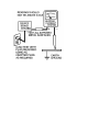
Specifications ComPair consists of a Windows based faultfinding program and an interface box between PC and the (defective) product. The ComPair interface box is connected to the PC via a serial or RS232 cable. In case of the EM1.1U chassis, the ComPair interface box and the TV communicate via a bi-directional service cable via the service connector at the rear side of the set (located at the left side of the rear cinch connectors, see also figure 1-2).
By a combination of automatic diagnostics and an interactive question/answer procedure, ComPair will enable you to find most problems in a fast and effective way. Beside fault finding, ComPair provides some additional features like: • Emulation of the (European) Dealer Service Tool (DST). • If both ComPair and SearchMan / Force (Electronic Service Manual) are installed, all the schematics and the PWBs of the set are available by clicking on the appropriate hyperlink.
7. Plug the AC power adapter in the AC power outlet and switch on the interface. The green and red LEDs light up together. The red LED extinguishes after approx. 1 second while the green LED remains lit. 8. Start ComPair and select 'File' menu, 'Open...' select 'EM1.1U Fault finding' and click 'OK'. 9. Click on the icon to switch 'ON' the communication mode (the red LED on the ComPair interface will light up). 10. Apply AC power to TV-set with the 'POWER' switch. 11.
Error Buffer Introduction The error code buffer contains all detected errors since the last time the buffer was erased. The buffer is written from left to right. When an error occurs that is not yet in the error code buffer, it is written at the left side and all other errors shift one position to the right. How to Read the Error Buffer Use one of the following methods: • On screen via the SAM (only if you have a picture).
Error Codes In case of non-intermittent faults, clear the error buffer before starting the repair. This is to ensure that 'old' error codes are not present. If possible, check the entire content of the error buffer. In some situations, an error code is only the result of another error code (and not the actual cause). For example, a fault in the protection detection circuitry can also lead to a protection. Table: Error Code Table Error Device Description Def.
Error Device Description Def.
Error 2 The HOP (pos. 7301 on diagram B4 detects the absence of an HFB pulse (pin 4 of connector 0324 on LSP, diagram A3)). A bit will be set in the HOP. After filtering by the software, the set will switch to protection mode. Error 3 This protection is activated when the high-tension voltage of the set is too high. It is called X-ray protection. This protection is triggered by circuitry around 3475 on diagram A3.
Error 5 See startup flow chart (figure 5.7). When POR bit is not communicated during startup, the processor will generate 'HOP POR not successful.' Error 6 This will occur in the following cases: § SCL or SDA is shorted to ground. § SCL is shorted to SDA. § SDA or SCL connection at the microcontroller is open. Error 7 Flash detection: From the EHT info, via D6303 and T7303, a flash will stop the H-drive and line output stage immediately. The FLS bit in the status register of the HOP is set to 'high.
Error 10 Non Volatile Memory (EEPROM - pos. 7012) does not respond to the microcontroller. Error 11 During the last startup, the NVM and the microcontroller did not recognize each other (e.g., one of them was replaced or the NVM memory has been changed/adapted or lost), therefore the NVM was loaded with default values. Error 12 Microprocessor (Painter - pos. 7001) internal RAM test failure. Error 13 Tuner (pos.
Error 31 SAA4978 PICNIC error (pos. 7709 on the SSB). Error 32 TDA 9330 HOP video control/geometry error (pos. 7301 on the SSB). Error 35 I/O expander IC M62320P I 2 C communication failure (pos. 7106 on the High Definition Jack panel). Note: Error codes 1, 2, 4, and 8 are protection codes, and in this case supplies of some circuits will be switched off. Also in protection, the LED will blink the number of times equivalent to the most recent error code.
Example of error buffer: 12 9 6 0 0 After entering SDM: § 1 long blink of 750ms followed by a pause of 1.5s, § 2 short blinks followed by a pause of 3s, § 9 short blinks followed by a pause of 3s, § 6 short blinks followed by a pause of 3s, § 1 long blink of 3s to finish the sequence, § the sequence starts again. Note : If errors 1, 2, 4 or 8 occur, the LED always gives the most recent error, even if the set is NOT in service mode. Protections General The EM1.
To get a quick diagnosis the EM1.1U has 3 service modes implemented: • The Customer Service Mode (CSM). • The Service Default Mode (SDM). Startup of the set in a predefined way. • The Service Alignment Mode (SAM). In this mode, items of the set can be adjusted via a menu and with the help of test patterns. The 'Protection Diagram' shows the structure of the protection system. See diagram below.
There are several types of protections: • I 2 C related protections (e.g., +5V supply check). • HOP related protections (mainly for deflection items). • Hardware errors which are not sensed by the Painter (e.g., BRIDGE_PROT) I 2 C Related Protections In normal operation some registers of the I 2 C controlled ICs will be refreshed every 200ms. During this sequence, the I 2 C busses and the I 2 C ICs as well will be checked.
• Flash detection. From the EHT info, via D6303 and T7303, a flash will stop the H-drive and line output stage immediately. The FLS bit in the status register of the HOP is set to 'high.' As the duration of a flash is very short, the FLS bit will be reset to 'low' again after the flash refresh and via a slow start the set will be started again.
General and Repair Tips General Figure: Start-up circuitry The startup of the set is very different from other sets (see figure 5-7 and 5-8): 1. When the set is switched 'on', first the HOP is placed in 'low power startup' mode (HOP standby mode). This means that 5V (derived from the available Standby supply) is connected to pin 22 of the HOP IC.
2. Now the HOP is driving the line circuitry with 50kHz pulses. At the base of the line transistor this is sensed via the 'STANDBY' line. 3. This signal triggers the Main supply to operate. Now the line stage has 'BAT' voltage (141 V); it will also start. 4. After the 5V and 8V supply lines are sensed by the Painter (via I 2 C), it will read the POR bit from the HOP via the I 2 C bus. 5. Now the HOP is switched into 'on' mode and the set will start up further with normal drive (31.468kHz for NTSC). 6.
Figure: Start-up diagram
Notice that a very big part of the set (Large Signal Panel) is 'hot,' meaning the primary part of the Standby supply, the whole Main supply (except for the secondary Audio supply), and the complete deflection circuit. So notice that the deflection-coil is hot. This set is not equipped with an IR transmitting LED. Instead, a Service (ComPair) connector is implemented at the rear of the set, which is directly accessible (not necessary to remove the rear cover).
5. Use a variac to slowly increase the AC power. Measure over sensing resistors R3514/15, to confirm a nice sawtooth voltage becomes available. Also measure the VBAT output. 6. VBAT may never exceed 141V. If so, there is something wrong in the feedback circuitry (e.g., regulator 7506). Caution: Be careful measuring the gate of FET 7504. Circuitry is very high impedance and can easily be damaged (first connect ground to measuring equipment, then measure the gate).
Vertical Deflection Caution: When you suspect the Vertical Deflection circuitry, please be careful. Because there is a DC voltage on the vertical deflection, the beam current can damage the CRT neck, leading to a defective CRT. The best thing to do is: 1. Interrupt pin 3 of connector 0224 on the CRT panel (diagram F), in order to remove the 'filament' voltage from the tube (no beam current, so no chance of destroying the CRT). 2.
Figure: Repair Tips
Alignments Contents of this chapter: • General Alignment Conditions • Hardware Alignments • Software Alignments and Settings Note: The Service Default Mode (SDM) and Service Alignment Mode (SAM) are described in chapter 5. Menu navigation is done with the “CURSOR UP, DOWN, LEFT or RIGHT” keys of the remote control transmitter.
Hardware Alignments Figure: Large Signal panel (LSP) Vg2 Adjustment Method 1 (without oscilloscope) 1. Connect a video pattern generator to the set with a “black pattern” signal. 2. First, adjust the Vg2 potmeter to the middle of the adjustment range. 3. Adjust the Vg2 potmeter of LOT (item 5430) to obtain a normal picture (without visible flyback lines).
Method 2 (with oscilloscope) 1. Connect the RF output (channel 3) of the pattern generator to the antenna input of the TV. Test pattern is a “black pattern” (blank screen on CRT without any OSD info). 2. Set Normal Red, Normal Green and Normal Blue to 32. 3. Set contrast to 0 and brightness to a minimum (with OSD still visible). 4. Set the channel of the oscilloscope to 50V/div. and the time base to 0.2ms.
Focus 1. Tune the set to a circle or crosshatch test pattern (use an external video pattern generator). 2. Adjust the first Focus potmeter (upper LOT potmeter, see figure 8-1) until the horizontal and vertical lines at 1/4 from east and west, at the height of the centerline, are of minimum width without visible haze. 3.
PIP AFC adjustment Set the pattern generator (e.g., PM5418) to a color bar video signal and connect the RF output to aerial input. Set amplitude to at least 1mV. 1. Connect a multimeter to the AFC output on pin 15 of IC 7914 (TDA9801). 2. Use potentiometer R3944 to adjust the AFC output to 2V6. Software Alignments and Settings General With the software alignments of the Service Alignment Mode, the Geometry, White tone and Tuner (IF) can be aligned. Put the set in the SAM mode (see chapter 5).
Figure: Geometry alignments
Alignments 1. Connect an external video pattern generator to the aerial input of the TV set with a crosshatch test pattern. 2. Use default settings as mentioned in paragraph 8.1. 3. Activate the SAM menu (see chapter 5). 4. Go to sub menu GEOMETRY. Now the following alignments can be performed: • Vertical slope (VER. SLOPE) Align the vertical center of the picture to the vertical center of the CRT. This is the first alignment to be performed of the vertical alignments. For an easy alignment set SERV.
• East West Trapezium (EW. TRAP) Align straight vertical lines in the middle of the screen. • East West Upper Corner (EW. UCORN) [*] Align straight vertical lines in the upper corners of the screen. • East West Lower Corner (EW. LCORN) [*] Align straight vertical lines in the lower corners of the screen. [*] Note: Perform these alignments also in 480p and 1080i mode (AV4). Use a 1080i pattern generator (e.g., Sencore VP300). When you leave the geometry menu, the values are stored.
Set the pattern generator (e.g., PM5418) to a white spot (chessboard) pattern and connect RF output with aerial input. Set amplitude to 1mV and use default settings as mentioned in paragraph 8.1. Alignment procedure: 1. NORMAL settings § NORMAL RED = 32 § NORMAL GREEN = 32 § NORMAL BLUE =32 2. COOL settings § DELTA COOL RED = -4 § DELTA COOL GREEN = 0 § DELTA COOL BLUE = +10 3. WARM settings § DELTA WARM RED = +10 § DELTA WARM GREEN = 0 § DELTA WARM BLUE = -6 4.
Peak-White Alignment You can adjust the light output of the CRT in the WHITE TONE sub menu. In this case, a color analyzer is necessary. 1. Set the pattern generator to a pattern having a white (100 % video) area and connect RF output to aerial input. Set amplitude to 1mV. 2. Set the default settings as mentioned in the start of this chapter. 3. Measure with a color analyzer (calibrated with the spectra) on the center of the white square on the screen.
Table: IF PLL offset AFA AFB IF PLL offset 0 0 Decrease offset value 0 1 Increase offset value 1 0 Correct 1 1 Correct AGC Set the pattern generator (e.g., PM5418) to a color bar video signal and connect the RF output to aerial input. Set amplitude to at least 1mV. Alignment procedure: 1. Enter SAM mode, select TUNER and activate the AGC line in the sub menu. 2. Connect a DC multimeter to pin 1 of the tuner (item 1200 on LSP). 3.
1. Enter SAM mode, select TUNER and activate the 2ND AGC line in the sub menu. 2. Connect a DC multimeter to pin 1 of the tuner (7201 on DW panel). 3. Adjust the 2ND AGC line until the voltage at pin 1 of the Tuner is just below 3.8V. 4. Increase/decrease the value by pressing the “CURSOR LEFT/RIGHT” button on the RC transmitter. 5. Store by pushing “MENU/SELECT”. 6. Switch the set to “STANDBY”. Option Settings Options are used to control the presence/absence of certain features and hardware.
Changes in the option byte settings are saved by leaving the OPTION submenu. Some changes will only take effect after the set has been switched off by breaking the AC mains supply (cold start).
Table: Option overview for type number 842 Byte Bit Abbr.
OB2 2 PIPT OB2 3 PIPC PiP Tuner PiP Control OB2 5 SOSD Smart OSD OB2 7 VDBY OB2 8 IPMU OB3 1 VCBK OB3 2 SPKC Program LiST Virtual DolBY Incredible Picture OB3 5 TIME OFF = function disabled / ON= OFF = function disabled / ON= function enabled OFF = full display of OSD not available / ON = available OFF = access to command is ignored / ON = access is processed OFF = Virtual Dolby not available / ON = Virtual Dolby is available OFF = INCR.
OB3 6 CCAP OB3 7 SURF OB3 8 VSLC Close OFF = function disabled / ON= Caption function enabled Surf OFF = function disabled / ON= slicing function enabled Control ON = Time window is set to 5s color delay OB4 4 AOUT Audio OUT OB4 6 ROTI OB4 7 BNUM OB4 8 VBNR function enabled OFF = Time Window is set to 2s / line OB4 5 TMWIN OFF = function disabled / ON= Auto Picture Selection OB4 3 INCF function enabled Vertical OB4 1 PAGC Picnic OB4 2 APC OFF = function disabled / ON= OFF = func
OB5 1 --- --- N/A OB5 2 --- --- N/A OB5 3 --- --- N/A OB5 4 --- --- N/A OB5 5 LTI Luminance Transient OFF = function disabled Improvement / ON= function enabled OB5 6 AKBL AKB Line OB5 7 CTSP Centre SPeaker OB5 8 VSR OFF = function disabled / ON= function enabled OFF = function disabled / ON= function enabled Vertical Scan OFF = function disabled Reference / ON= function enabled OB6 1..8 N/A (RESERVED) N/A OB7 1..8 N/A (RESERVED) N/A OB8 1..
Byte Bit Abbr.
Byte Bit Abbr. Feature Description (OFF = 0, ON = 1) OFF = Virtual Dolby not OB2 7 VDBY Virtual DolBY available / ON = Virtual Dolby is available OFF = INCR.
Byte Bit Abbr.
Circuit Descriptions and Abbreviation List Index of this chapter: 1. Introduction. 2. Block diagram. 3. Power Supply. 4. Control and Teletext. 5. Tuner and IF. 6. Video: HD Jack Interface (AV4, 1080i/480p). 7. Video: High-end Input Processor (HIP). 8. Video: Feature Box (FBX). 9. Video: High-end Output Processor (HOP). 10. Video: 3D-Comb filter. 11. Synchronization. 12. Horizontal Deflection. 13. Vertical Deflection. 14. Audio. 15. CRT and SCAVEM. 16. Double Window (DW). Introduction The EM1.
The user interface and micro controller are the same as used in the H8 set. In the N8 however, a HIP, PICNIC, and HOP are used for the '100 Hz' function i.s.o. the BOCMA in the H8. The HIP and HOP have about the same functionality as the BOCMA. This chip set however, sees to it that line frequency and YUV-signals are doubled (2 fh), while the vertical frequency stay 60 Hz (1fh).
Note: The start-up behavior of the N8 is different than that of the MG-chassis, meaning that the 'Supply ON/Deflection OFF' situation does not exist. This means that isolating failures in the N8 must be done in a different way. See Chapter 5 of this manual.
The tuner type is a PLL tuner and delivers the IF-signal, via audio and video SAWfilters, to the HIP (High-end Input Processor). The HIP has the following functions: • IF modulation. • Video source - and record select. • Color decoder. • Synchronization. Five video in/output connections (with audio connections) are available: 1. Front: interfaces CVBS 2. AV1: interfaces CVBS and YUV-input (1fH) 3. AV2: interfaces CVBS and Y/C (meant for VCR-connection) 4. AV4: interfaces YPbPr/RGB (HD) inputs (2fH).
signals from CC/OSD are also inserted via the HOP. The video part delivers the RGB signals to the CRT-panel and the geometry part delivers the H-drive, V-drive, and a drive-signal for rotation (as a variable DC-level on the V-drive signal). Both deflection circuits are 'hot' and located on the LSP and are driven by the HOP. To make the galvanic separation, the line drive is driven via transformer 5410 and the frame drive via optocoupler 7610.
The difference between this and former MG-sets is that VBAT is not mains isolated ('hot') and is alignment free. Power Supply (Diagram A1 and A2) General The power supply has a number of main functions.
C2507 prevents the high-frequency signals, generated by the set, to be conveyed into the mains by short-circuiting them. In the case of a lightning surge between the two phases (differential mode), the energy is immediately bled away through the VDR (R3509) to the other phase. In case of a lightning surge on both phases of the mains in relation to the aerial earth, the mains filter acts as a high resistance (UEMK=L * dI/dt) as a result of which the voltage across coil L5504 increases.
Standby Power Supply (Diagram A2) This power supply is of a SOPS type (Self-Oscillating Power Supply) and is regulated by the controlled switching of an oscillator. It uses the so-called 'Flyback' principle: Figure: Flyback principle • After closing switch 'S', the current ID will increase linearly in time. The magnetic energy in the primary coil is directly proportional with the self-inductance of the coil and current ID (thus with time the switch is closed).
Figure: Standby supply circuitry To apply this on the N8 (diagram A2): replace switch 'S' by FET TS7102, coil L by L5101, diode D by D6111 and C by C2104. Time interval t0 - t1: After switching the set on, the gate of MOSFET TS7102 will be high (max. 15V due to zener diode D6105). This will drive the FET into saturation (UDS = 0V). The DC-voltage UMAINS will be transposed across the primary winding of L5101 (Pins 3 & 5) resulting in a linearly increasing current through this coil.
The maximum current is determined by the time the FET stays into conductance (t0 t1). This time is directly determined by the voltage across R3108//R3118. This voltage is a measure of the current and if it exceeds 1.4 V, TS7101 will be driven into conductivity and consequently connect the gate of TS7102 to ground; the FET will block. The voltage across the secondary winding (Pins 8 & 9) will be negative, diode D6111 will block.
Transistor TS7100 will be driven and a negative voltage will be transposed to the emitter of TS7101. When TS7101 conducts, the gate of the FET is at earth potential, forcing the oscillator to stop. Due to the load, the secondary voltage UOUT will decrease. At a certain voltage, optocoupler TS7104 will block and the oscillator will start again. Since there are no capacitors and there is a high amplification-factor in the feedback circuit, the feedback is ultra-fast. This is why the ripple on UOUT is minimal.
Main Supply (Diagram A1) Some important notes on beforehand: • VBAT is not isolated from the main supply ('hot'). • VBAT is alignment free. The Main Power Supply generates the 141 V (VBAT) and the 28 V for the audio part, and is based on the so-called 'down converter' principle.
• After closing switch 'S', the linear in time increasing current IT, , will charge capacitor C. • Opening switch 'S' will generate a counter-e.m.f. in coil L, trying to maintain current IT. This is possible via diode D (this diode is also called 'freewheel diode'). So after opening 'S', the magnetic energy stored in coil L will be transferred to electrostatic energy in capacitor C. The VIN will only supply current during the time that 'S' is closed while a constant current is flowing through RL.
At start-up of the main supply, C2515 can be assumed as being a short-circuit. UAB will be 15 V (R3513, D6510) and UGS of the FET will be +5.4 V (voltage division over R3512 and R3518). The FET will be driven into saturation (same as closing switch 'S'). The drain-current will increase linear in time. With other words: resistors R3513 and R3518 will start the oscillator. The voltage across the co-coupled coil (4, 5) is also positive and will keep the FET into conductivity.
Via a voltage divider, existing of (1 %) resistors R3507, R3510 and R3527, a voltage of 2.5 V (when VBAT = 141 V) is fed to the input of precision shunt regulator 7506. This regulator will conduct, a current will flow through R3524, and TS7505 will be driven into conductivity. The base of TS7502 will now be set at a certain positive voltage. As this transistor switches the FET TS7504 on and off, this circuit can determine the duty-cycle. E.g. when the load increases, VBAT will decrease.
If, for any reason, the stabilization circuit fails, the output voltage VBAT can never exceed 200 V (via D6514). D6514 will form a short-circuit, VBAT will drop and the set will switch off (this will result in an audible hiccupping of the supply). Set to 'POWER OFF' (via RC): When the set is switched to 'POWER OFF' via the Remote Control, the Main supply will be switched off.
Guarding circuit: The 11V of the line-stage is monitored. The +28V winding (pin 6) of supply-transformer 5506 is monitored. (These pulses, when switching off the set, exist longer than the 11V-level) When switching off the set by the 'POWER'-switch, the 11V will decrease and will generate a positive STAND-BY (POR) pulse. At that moment the RGB-outputs will be driven such that the EHT-capacitor is heavily loaded in order to have a nice switch off spot.
Control and Closed Captioning (diagram B7) Painter The SAA5677/M1 (IC7001) is called the Painter (OSD, CC and Control). In this IC, the microprocessor and the Closed Captioning-decoder are integrated. Some of its functions are: • Set control. • CC/OSD acquisition. • RGB-outputs to the HOP • I/O-ports for I2C, RC5, LED, and service modes. • Error code generation. The software for N8 can be 192kB. The Non Volatile Memory IC7011 is a 4kB version M24C32. All ICs in this part are supplied with 3V3.
Closed Captioning The painter deals with CC-decoding. The Painter gets its video signal directly on pin 31 (from the HIP). The RGB-outputs are available on pins 46/47/48. Fast blanking is realized via pen 52. I2C In the N8-chassis with Painter-processor there are two I2C-busses used: • Slow (max. 100 kHz) hardware I2C-bus (called I2C1) used for all IC communication. • Separate short bus (called I2C 3) for the Non Volatile Memory (NVM) to avoid data corruption.
Tuner and IF (Diagram A7 and B2) The tuner is I2C-controlled and is capable of receiving off-air and cable channels: The tuning is done via I2C. The reference voltage on pin 9 is 33 V. This voltage is derived from the 180 V (from the LOT) via two resistors of 2.2k ohm (diagram F). The Painter together with the HIP controls the tuning procedure. The IF-filter is integrated in a SAW (Surface Acoustic Wave) filter. Two SAW filters are used: One for filtering picture-IF and one for filtering sound-IF.
Video: HD Jack Interface (Diagram N) The Jack High Definition module covers the following functions: 1. RGB output selection. 2. Matrix circuit to convert YPbPr to RGB. 3. Sync slicer for YPbPr sync on Y, RGB sync on Green. 4. Sync selection. 5. Control Function. 6. Audio feed-through of signal source.
RGB Output Selection The module has two video inputs and one RGB output (going into the set.) The inputs can also handle 1080i-signals and 480p-signals (both in RGB format and YPbPr format.) (This selection circuitry is also needed to cope with the various formats of the nonstandardized HD set top box business.) Video-input (3 cinches, reference number 1993-A-B-C): • YPbPr with sync on Y. • RGB with sync on green (note: cinch-inputs are normally used for YPbPr input.
Sync Slicer The sync slicer extracts the horizontal and vertical synchronization signals for the HOP (in the set): • From the 3-level sync pulses Y of the 1080i YPbPr • From the 3-level sync pulses Green of the 1080i RGB • From the normal sync pulses of the 480p signal Explanation of 3-level sync shown in picture: Figure: 3 level sync Example of a 2-level sync pulse: CVBS-signal with two levels of sync (-300 mV, 0 mV) Example of a 3-level sync pulse: ATSC-signal with three levels of sync (-300 mV, 0
Sync Selection If the synchronization is derived from Y or Green, the H and V sync from the sync-slicer must be selected. • When YPbPr-signal or RGB-signal is 480p-format: sync signals will be V-770 and H-770-2 sync. • When YPbPr-signal or RGB-signal is 1080i-format: sync signals will be V-770 and H-770-3 sync. When the sync is separate (H and V), the sync of the source must be selected. The IO-4, IO-5 control-lines select the sync-inputs of the HEF4052 (7102.
Video: High-end Input Processor (HIP, diagram B2) In the N8 the TDA932xH input processor is used, which contains the following functions: • IF demodulation. • AFC signal generation, used to track drifting transmitters. • Sound carrier re-generation (SIF). • Sync acquisition, delivering HA and VA. • Switching off IF-filtering. The HIP has various inputs.
Video Processing The sandcastle-pulse of the HIP will not be used for synchronization. The HOP will generate synchronization signal derived from the feature box (PICNIC) signals. The HIP itself (no external voltage) controls the Y/C switch in the HIP. The Chrominance decoder in the HIP is full multi-standard, but only NTSC is decoded. One crystal is connected to the pin 57 without any alignment. The crystal is also used as a reference for the synchronization.
ADC/DAC Analogue to Digital conversion is done with three identical 9-bit ADC's. Digital to Analogue conversion uses three identical 10-bit DACs. In the PICNIC there are three 9 bits ADCs present for Y, U and V. For digitizing the Y (luminance) 9 bits are used, to realize a more detailed picture. The nine bits are only used internally. Via dithering, the nine bits are reduced to eight bits and that data is stored in memory.
CTI At CVBS video signals, the bandwidth of color signals is limited to 1/4 of the luminance bandwidth. Transients between areas of different color are therefore not very sharp. The PICNIC can increase these transients artificially with a time manipulation algorithm. Dynamic Contrast To make the contrast (black/white) range wider, Philips has invented Dynamic Contrast. It uses the digital memory used in digital scan sets.
PROZONIC Figure: 100 Hz conversion To the PICNIC, external ICs are connected dependent of the features. For N8-sets with Digital Scan the PROZONIC (IC7708, SAA4990H) is placed with two memory ICs (IC7714 and 7715). It is an abbreviation for PROgressive scan ZOom and Noise reduction IC. When applying this, the second Field Memory has to be installed.
• Line flicker reduction (Digital Scan): this is a feature to reduce the 30 Hz interlace line flicker. • Dynamic Noise Reduction: noise affected signals can be improved by combining the pixel values of the current and past video fields. This is however only possible in areas without movement.
Video Control After conversion to RGB again, the signals can be controlled for Saturation, Contrast, and Brightness. 2nd RGB Interface for OSD/CC On pins 35 to 38, the RGB and fast blanking from the Painter (OSD and CC) are inserted. Peak White Limiting On pin 43 there is a Peak White Limiting signal line (PWL). If the beam current (EHTinfo line) increases, then the EHT-info voltage will decrease. PWL is controlled by average limiting via R3343/C2333. Cut-off Control Switching the TV to Standby: 1.
In this chassis, a 'one-point' cut-off control is used: A current of 8A (for cut-off) is fed to pin 44 of the HOP. This is done with a measurement pulse during the frame flyback. During the first frame, three pulses are generated to adjust the cut-off voltage at a current of 8A. With this measurement the black level at the RGB-outputs is adjusted. So at start-up there is no monitor pulse anymore. At start-up, the HOP measures the pulses, which come back via pin 44. The RGBoutputs have to be between 1.
East/West Drive. At pin 3, the E/W-drive is available. Pin 4 is a feedback input for the EHT-info and is used to prevent pumping of the picture. EHT varies also dependent of the beam current. Frame Rotation. For frame rotation, a control voltage is used from pin 25 of the HOP. This voltage can vary from 0.4V to 4V. Guarding Protections: Flash detection: When a flash occurs, the EHT-info will become negative very fast. Via D6303/D6304/R3316, TS7303 starts to conduct. This makes pin 5 of HOP high.
3D Comb Filter (Diagram CO) Conventional Comb filters separate the luminance (black and white picture information) from the chroma (color picture information), by comparing horizontal scanning lines within one video frame The 3D Digital Comb Filter takes this idea two steps further by acting upon not only consecutive lines within the frame, but in the frame before and after as well. The added analysis and correction result in far sharper pictures with less noise, as well as an enhanced purity of color.
Figure: Block diagram 3D Comb panel Synchronization (Diagram B3 and B4) The HIP video processor provides vertical and horizontal sync pulses VA and HA, which are synchronized with the incoming CVBS signal. These pulses are fed to the PICNIC where they are doubled to be synchronous with the 100Hz picture. The outgoing pulses, VD100 (in reality 60 Hz), and HD100 are fed to the HOP that supplies the vertical and horizontal drive pulses and the 2fH sandcastle pulse.
The 'framedrive +' line drives the frame deflection. When no CVBS is offered to the video processor, the VA and HA pulses are switched 'off' by the HIP, and the VD and HD pulses are then generated by the PICNIC. This to assure a stable OSD. This also counts for the AV4 input signal (HD input). When having no signal here, we still have a stable OSD.
The HOP (located on the SSB) generates the line-drive pulses (LINEDRIVE1), which have a frequency of 31468 Hz (T = 31.77s). When the LINEDRIVE1 signal is high, TS7409 and TS7408 will conduct. A constant DC voltage will be applied across L5410, causing a linear increasing current through this coil. The secondary voltage of L5410 has a negative polarity so that TS7421 will block.
Operation of the Line Output Stage To explain the operation of the line output stage, we use the following start conditions: • C2433 is charged to max. 141 V (VBAT) • TS7421 is driven into conductivity. Figure: Line deflection part 1 Period t1 - t2: When TS7421 is driven into conductivity, the capacitor voltage of 141 V will be divided across bridgecoil L5422 and the deflection coil (conn. 0317). Due to the chosen inductance values, there will be 100 V across the deflection coil and 41 V across L5422.
through L5422 continues to flow through C2426 and C2421. The energy stored in the line deflection coil is passed to C2425, and the energy of L5422 to C2426. The resonance-frequencies of these two LC-circuits define the flyback time of the spot from the right side of the picture tube to the left. On average, no current flows through C2421 and thus the voltage across this capacitor remains constant.
The Linearity Correction A constant voltage across the horizontal deflection coil should result in a linear increasing saw-tooth current. This however is not the case as the resistance of the coil is not negligible. In order to compensate for this, a pre-magnetized coil L5421 in series with the deflection coil is used. This coil ensures that during time interval t1 - t3 the circuit-resistance will be higher than during t4 - t5. L5421 is called the linearity coil.
The E/W-Correction A line, written at the upper- or lower side of the screen, will be larger at the screen center when a fixed deflection current is used. Therefore, the amplitude of the deflection current must be increased when the spot approaches the screen center. This is called East/West correction. The EW-DRIVE signal is generated in the HOP and will drive FET TS7480 via TS7481 and optocoupler TS7482.
The DYN-FASE-CORR signal is fed to the HOP via C2455 and drives a dynamic phase correction necessary because of beam current variations. This is done by regulating TON of the line transistor TS7421. East-West Circuit The moment TS7480 is driven into saturation, C2421 will discharge during the flyback. As a consequence of which C2421 must be charged again during the scan via the conduction diode D6422 (as long as C2421 is not charged to the voltage across L5422, D6422 will conduct).
• EW-corner, • EW-trapezium, • Horizontal parallelogram, • Horizontal bow. Beam Current Correction The EHT-info at point 10 of the LOT is dependent on the value of the beam current and the voltage divider R3450, R3451, and C2450. The EHT-info is fed to the HOP to trim the contrast and to compensate for the changes in picture-width as a function of the EHT-info, when the high-voltage is decreased.
The HOP drives the frame output stage. As the HOP is 'cold' and the frame output stage is 'hot', they must be galvanic isolated. This is done by means of an optocoupler. In the MG-chassis, the HOP generates three signals needed for the frame output stage: VDPOS, VDNEG and FRAME ROTATION. To avoid the costs of three optocouplers, the frame drive pulse and rotation DC-voltage are added together and then fed to optocoupler TS7610.
The sawtooth voltage for the frame output stage is not generated by the HOP but by a discrete circuit after the optocoupler 7610 via R3600 and R3601 a linear increasing voltage over C2601 is built up with a large time constant. The circuit around TS7603 is a current source, driving C2601 with a current value derived from the E/W modulator. This will result in an S-shaped voltage on C2601 (also known as EW-correction).
Protection Circuit for Bridge-Coil and Frame Output Stage The secondary voltage of bridge coil L5422 is guarded at the diode modulator (D6421/22) via a detection circuit consisting of an 8.2 V zener diode (6499 on diagram A3). When the bridge-coil is working properly, the average voltage on D6422 is such that this zener diode will conduct and will drive TS7652 into saturation via the BRIDGE_PROT signal (see diagram A4).
All MSP versions contain digital audio processing used for the basic left/right stereo sound, such as bass, treble, balance, incredible sound and spatial. In addition to that, the MSP3451 is also able to perform Virtual Dolby; a Dolby approved sound mode for surround sound reproduction with left/right speakers only. The MSP3451 is capable of supporting four stereo inputs. Therefore, an extra input selector (HEF4052) is not needed.
Explanation BTSC Stereo System (USA) The standard for TV stereo audio in the USA was set by the Broadcast Television Systems Committee (BTSC). The BTSC system was designed to: • be compatible with then current monaural TV receivers, • present a good stereo separation and signal to noise ratio, • make available a Second Audio Program as a separate audio channel, • provide a technical voice/data channel to communicate within the TV stations system.
The figure also shows the Second Audio Program (SAP) frequency, which is a constant carrier of an audio tone of 5fH (78,670 Hz), FM modulated by the SAP program content. SAP is always monaural. The material on the SAP audio may, in some cases, not be related to the video content. Alternatively, it may contain a verbal description of the action in the video for those who can not view the picture. Some stations use it to transmit background music or book reading for the blind.
Audio Processing The sound processing in N8 is completely done by the MSP3451G for 'Virtual Dolby' sets: • Volume control is done by the user via the SOUND menu. • Tone control is done via the BASS/TREBLE control. • Headphone control : In 'Virtual Dolby'-sets, the MSP has a separate Headphone output so separate sound control is possible. • Mute control can be done in different ways: § Via the 'SOUND_ENABLE' line of the Painter.
Audio Amplification The audio amplifier part is very straightforward. It uses two integrated power amplifiers (TDA2616). It delivers an output of 2 x 10WRMS to two full range speakers and/or subwoofer. The supply voltage is +28 V, generated by the main supply via L5506. Muting is done via the 'SOUND-ENABLE' line connected to pin 2 of the amplifier IC and coming from the Painter.
At the end of the slope, the SCAVEM-current decays to zero, and the spot is at the original position. An overshoot occurs which improves the impression of sharpness. At the negative slope, the SCAVEM-current counteracts the deflection. During the first half of the slope, the spot is delayed and the slope becomes steeper. During the second half the spot accelerates, the SCAVEM-current is zero at the end of the slope.
Key Components: • Tuner (1900): UV1336BL9/AGS • SAW Filter (1901): OFWM1962M • IF processor (7914): TDA9801 • PIP processor (7803): M65669 • Switching ICs: TDA8601 (7919), HEF4053 (7801 & 7916) • IO expander (7403): M62320P
Block Diagram: There are basically two types of configurations. 2-antenna inputs or one tuner PIP, as shown in Fig. 1.
Circuit Descriptions IF section (for set with 2-antenna inputs) Basically the IF-processing works around IC7901 TDA9801 and tuner. It demodulates the IF signal received from the tuner at pin-1 & 2 via SAW filter 1901, processes it into CVBS signal and outputted at pin-7. The AGC and phase alignments are possible on this panel.
In order to display the external AV sources by the PIP panel, source selection circuit is incorporated on the panel. In A10 PIP execution, 3 external AV sources are possible (AV1, AV2/S-VHS1, AV3/S-VHS2). The selection between these sources is done by IC7801 HEF4053. Note: When S-VHS is inserted from the rear, AV2 source will be disabled. Likewise when S-VHS is inserted from the side-AV. The switching logic of AV sources is shown in Table-2.
DACs. The YUV are output at pin-39, 37 & 35 of IC7803 respectively. In order to display the PIP sub-picture correctly on the main picture, the VFB & SANDCASTLE sync signals from the deflection are connected to IC7803 pin-33 & 32. The sub-picture YUV signals are fed to fast switching IC7919 TDA8601 pin-6, 7 & 8. In normal operation (w/o PIP), the main picture YUV signals ( at pin-2, 3 & 4) are bypassed by IC7919, and returned back to the main video processor.
Table: Semi-standby switching logic Condition Normal Semi Stdby pin Stand By pin 12 IC7910 13 on main uP High High Remarks PIP ON, TV ON,Main Front End ON PIP OFF, TV Stand By Low Low OFFMain Front End OFF Semi Stdby PIP OFF, TV Low High OFFMain Front End ON Power Supply The power supplies used by PIP panel are from the main board 5V, 8V and 33V (for tuner only). The 5V is supplied to tuner 1900, VIF IC7914 and switching circuitry of IC7801 & IC7916.
Abbreviation List Abbreviation Description 1fh 1 time the line frequency 2fh 2 times the line frequency 480p 480 lines resolution (progressive scan) 1080i 1080 lines resolution via interlacing AARA Automatic Aspect Ratio Adaptation: algorithm that adapts aspect ratio to remove horizontal black bars; keeping up the original aspect ratio ADC Analogue Digital Converter AFC Automatic Frequency Control: control signal used to tune to the correct frequency AGC Automatic Gain Control: algorithm th
AUDIO-R Audio Right AUDIO-SL Audio Surround Left AUDIO-SW Audio Subwoofer Auto TV Name for the combination of picture features/improvements, which work automatically (ANR/Auto sharpness/Auto Histo/ambient light).
CRT Cathode Ray Tube or picture tube CSM Customer Service Mode CTI Color Transient Improvement: manipulates steepness of chroma transients CVBS Composite Video Blanking and Synchronization CVBS-SC1-IN CVBS EXT1 in CVBS-SC2 OUT CVBS EXT2 out CVBS-SC2-IN CVBS EXT2 in CVBS-SC3-IN CVBS EXT3 in CVBS-SC4-IN CVBS EXT4 IN CVBS-TER CVBS terrestrial CVBS-TXT-OUT CVBS teletext out CVBS-Y-FRONT CVBS luminance front input DAC-HOP Digital analogue converter HOP IC DC-filament Filament supply vo
DSP Digital Signal Processing DVD Digital Versatile Disc DW Double Window DYN-FASE-COR Dynamic phase correction EHT Extra High Tension EHT-INFO Extra High Tension information EW East West, related to horizontal deflection of the set EXT External (source), entering the set via EXT or via cinches FBL Fast Blanking: DC signal accompanying RGB signals FBL-SC1-IN Fast blanking signal for EXT1 in FBL-SC2-IN Fast blanking signal for EXT2 in FBL-TXT Fast Blanking Teletext FBX Feature Box: p
G-SC1-IN Green EXT1 in G-SC2-IN Green EXT2 in H-770-2 Horizontal 2 level sync pulse (HD-sources) H-770-3 Horizontal 3 level sync pulse (HD-sources) HA Horizontal Acquisition: horizontal sync pulse coming out of the HIP HD100 Horizontal Drive: horizontal sync pulse coming out of the featurebox HD-input High Definition (2fh) input of AV4 HDTV High Definition TV: highest resolution defined by the ATSC standard (1080 lines and 1920 horizontal pixels, referred to as 1080i) HEATER Heater (Filamen
IN-FRONT-SNDL Sound left front in IN-FRONT-SNDR Sound right front in IN-SC1-B In EXT1 Blue IN-SC1-G In EXT1 Green IN-SC1-R In EXT1 Red IN-SC1-SNDL In EXT1 sound left IN-SC1-SNDR In EXT1 sound right IN-SC2-B In EXT2 Blue IN-SC2-CVBS_Y In EXT2 CVBS or luminance (SVHS) IN-SC2-FBL In EXT2 fast blanking IN-SC2-G In EXT2 Green IO-BUS In/Out - Bus Last Status The settings last chosen by the customer and read and stored in RAM or in the NVM.
MUTE Mute-Line NC Not Connected NDF No vertical Deflection: vertical fly back protection NHF No Horizontal deflection: horizontal fly back protection NVM Non Volatile Memory: IC containing TV related data e.g.
frame at the same time, creating a double vertical resolution.
SLDP Smart Local Dooming Prevention (HW and SW) SMC Surface Mounted Components SNDL-SC1-IN Sound left EXT1 in SNDL-SC1-OUT Sound left EXT1 out SNDL-SC2-IN Sound left EXT2 in SNDL-SC2-OUT Sound left EXT2 out SNDR-SC1-IN Sound right EXT1 in SNDR-SC1-OUT Sound right EXT1 out SNDR-SC2-IN Sound right EXT2 out SNDR-SC2-OUT Sound right EXT2 out SNDS-VL-OUT Surround sound left variable level out SNDS-VR-OUT Surround sound right variable level out SNERT Synchronous No parity Eight bit Recept
YPbPr YUV-input with other naming YUV YUV-input C Micro controller V-100 V from Feature Box V-770 Vertical synchronization (HD-sources) VA Vertical Acquisition Vbat Main supply for deflection (mostly 141 V) Vchip Violence chip (used in DW-module) VD100 Vertical Drive: vertical sync pulse from deflection VFB Vertical Fly back Pulse: vertical sync pulse coming from the feature box VSYNC Pulse derived of 530 s-circuit behind the HOP, to vertically synchronize the Painter VL Variable Leve
EM1.
EM1.
EM1.
EM1.
EM1.
All Models (7644) - Chassis Overview
All Models (7644) - Main Supply [A1]
All Models (7644) - Stand-by Supply [A2]
All Models (7644) - Line Deflection [A3]
All Models (7644) - Frame Deflection/Rotation [A4]
All Models (7644) - Audio Amplifier [A5]
All Models (7644) - Headphone Amplifier [A6]
All Models (7644) - Tuner, I/O, SIMM Connector [A7]
All Models (7644) - Front [A8]
All Models (7644) - Sim Connector (Male) [B1]
All Models (7644) - IF, I/O Video Processing [B2]
All Models (7644) - Feature Box [B3]
All Models (7644) - HOP [B4]
All Models (7644) - Audio Demodulator [B6]
All Models (7644) - Painter [B7]
All Models (7644) - 3D Comb [CO]
USED ONLY IN MODELS: 32PT842H37A, 36PT842H37D (7644) - PIP 2ND Front-end [C1]
USED ONLY IN MODELS: 32PT842H37A, 36PT842H37D (7644) - PIP Colour [C2]
All Models (7644) - Side I/O Panel [D]
USED ONLY IN MODELS: 27PT830H37C, 32PT830H37A (7644) - Top Control Panel PV0 Styling [E]
USED ONLY IN MODELS: 32PT842H37A, 36PT842H37D (7644) - Top Control Panel PV2 Styling [E]
All Models (7644) - CRT PANEL [F]
NOT USED IN MODELS: , 32PT740H37A (7644) - DC Shift Panel [G]
NOT USED IN MODELS: , 32PT740H37A (7644) - VDAF Panel + 2nd Orders [I]
NOT USED IN MODELS: , 32PT740H37A (7644) - Front Interface Panel (For PV0 & PV2 Styling) [J]
USED ONLY IN MODELS: 32PT740H37A (7644) - Front Interface Panel (For SL3 Styling) [J]
NOT USED IN MODELS: , 32PT842H37A, 36PT842H37D (7644) - Control (For no PIP) [N1]
NOT USED IN MODELS: , 32PT842H37A, 36PT842H37D (7644) - Inputs / Outputs (For no PIP) [N2]
NOT USED IN MODELS: , 32PT842H37A, 36PT842H37D (7644) - Sync Slicer (For no PIP) [N3]
NOT USED IN MODELS: , 32PT842H37A, 36PT842H37D (7644) - Matrix (For no PIP) [N4]
USED ONLY IN MODELS: 32PT842H37A, 36PT842H37D (7644) - Control (For PIP) [N1]
USED ONLY IN MODELS: 32PT842H37A, 36PT842H37D (7644) - Inputs / Outputs (For PIP) [N2]
USED ONLY IN MODELS: 32PT842H37A, 36PT842H37D (7644) - Sync Slicer (For PIP) [N3]
USED ONLY IN MODELS: 32PT842H37A, 36PT842H37D (7644) - Matrix (For PIP) [N4]
All Models (7644) - YPbPr [Q]
All Models (7644) - Layout LSP (Top Side)
All Models (7644) - Layout LSP (Bottom Side)
All Models (7644) - Layout SSB (LOT Side)
All Models (7644) - Layout SSB (Tuner Side)
All Models (7644) - Layout 3D Comb (Top View)
All Models (7644) - Layout 3D Comb (Bottom View)
USED ONLY IN MODELS: 32PT842H37A, 36PT842H37D (7644) - Layout PIP Panel (Top Side)
USED ONLY IN MODELS: 32PT842H37A, 36PT842H37D (7644) - Layout PIP Panel (Bottom Side)
All Models (7644) - Layout Side I/O Panel (Top Side)
All Models (7644) - Layout Side I/O Panel (Bottom Side)
USED ONLY IN MODELS: 27PT830H37C, 32PT830H37A (7644) - Layout Top Control Panel PV0 Styling (Top Side)
USED ONLY IN MODELS: 27PT830H37C, 32PT830H37A (7644) - Layout Top Control Panel PV0 Styling (Bottom Side)
USED ONLY IN MODELS: 32PT842H37A, 36PT842H37D (7644) - Layout Top Control Panel PV2 Styling (Top Side)
USED ONLY IN MODELS: 32PT842H37A, 36PT842H37D (7644) - Layout Top Control Panel PV2 Styling (Bottom Side)
All Models (7644) - Layout CRT Panel (Top Side)
All Models (7644) - Layout CRT Panel (Bottom Side)
NOT USED IN MODELS: , 32PT740H37A (7644) - Layout DC Shift Panel
NOT USED IN MODELS: , 32PT740H37A (7644) - Layout VDAF + 2ND Order Panel (Top Side)
NOT USED IN MODELS: , 32PT740H37A (7644) - Layout VDAF + 2ND Order Panel (Bottom Side)
NOT USED IN MODELS: , 32PT740H37A (7644) - Layout Front Interface Panel (For PV0 & PV2 Styling) (Top Side)
USED ONLY IN MODELS: 32PT740H37A (7644) - Layout Front Interface Panel (For SL3 Styling) (Top Side)
NOT USED IN MODELS: , 32PT842H37A, 36PT842H37D (7644) - Layout Jack High Definition Interface Panel (For no PIP) (Top Side)
NOT USED IN MODELS: , 32PT842H37A, 36PT842H37D (7644) - Layout Jack High Definition Interface Panel (For no PIP) (Bottom Side)
USED ONLY IN MODELS: 32PT842H37A, 36PT842H37D (7644) - Layout Jack High Definition Interface Panel (For PIP) (Top Side)
USED ONLY IN MODELS: 32PT842H37A, 36PT842H37D (7644) - Layout Jack High Definition Interface Panel (For PIP) (Bottom Side)
All Models (7644) - Layout YPbPr (Top Side)
All Models (7644) - Layout YPbPr (Bottom Side)
All Models (7644) - Testpoint Overview LSP
All Models (7644) - Testpoint Overview SSB
All Models (7644) - Testpoint Overview CRT Panel
27PT830H37C - Manual no. 7644 Large Signal Panel Large Signal Panel CBA Large Signal Panel . . . . . . . . . . S 0010 2 Pin Board Connector. . . . . . . . . S 0020 2 Pin Board Connector. . . . . . . . . 0150 Fuse Holder. . . . . . . . . . . . . . 0153 Fuse Holder. . . . . . . . . . . . . . 0203 4 Pin Board Connector. . . . . . . . . 0204 6 Pin Board Connector. . . . . . . . . 0317 2 Pin Board Connector. . . . . . . . . 0324 7 Pin Board Connector. . . . . . . . . 0325 3 Pin Board Connector. . . . . . . . .
27PT830H37C (continued) S S S S S S S S S S S S S S S S S 2926 2927 2928 2941 2942 2951 2952 2953 3101 3102 3103 3104 3105 3106 3107 3108 3109 3110 3113 3114 3117 3118 3119 3120 3121 3123 3124 3125 3126 3127 3130 3148 3200 3201 3202 3203 3230 3237 3402 3403 3404 3406 3407 3408 3409 3410 3411 3414 3415 3417 3418 3431 3436 3450 3451 3452 3454 3455 3458 3459 3460 3461 3462 3463 3464 3465 3466 3467 3468 3470 3471 3472 3473 3474 3475 3476 3477 3478 3479 3481 3484 3485 3486 3487 3489 3490 3495 3496 3497 3
27PT830H37C (continued) 3705 3706 3710 3711 3714 3715 3716 3717 3730 3731 3732 3733 3734 3735 3736 3737 3738 3739 3740 3741 3742 3743 3744 3745 3750 3756 3757 3758 3762 3765 3770 3773 3789 3790 3792 3908 3909 3910 3911 3912 3913 3914 3915 3919 3920 S 3925 3928 3929 3930 3932 3935 3936 3937 3940 3941 3944 3946 3950 3955 3970 3971 3972 3975 3991 3992 3993 3995 3996 3997 4102 4401 4402 4403 4405 4406 4407 4408 4409 4410 4412 4413 4415 4416 4441 4442 4443 4444 4483 4521 4522 4611 4619 Res, Res, Res, Res, Res,
27PT830H37C (continued) 6422 6436 6437 6442 6451 6452 6453 6454 6456 6461 6463 6465 6466 6468 6480 6481 6482 6492 6493 6499 6505 6506 6507 6508 6510 6511 6512 6513 6514 6515 6516 6517 6518 6519 6600 6616 6619 6620 6623 6636 6660 6665 6731 6732 6900 6901 6902 6903 6904 7100 7101 7102 7103 S 7104 7228 7407 7408 7409 7421 7440 7452 7480 7481 S 7482 7501 7502 7504 7505 7506 7510 7528 7529 7600 7602 7603 7605 7606 S 7610 7620 7640 7641 7652 7653 7654 7655 7702 7720 7721 7722 7723 7724 7725 Diode, Rect, BY229X-6
27PT830H37C (continued) 9904 9906 9907 9908 9909 9910 9911 9912 9914 9916 9917 9920 9921 9922 9925 9926 9927 9928 9931 9932 9933 9934 9936 9943 9944 9945 9946 9947 9948 9950 9951 9952 9957 9958 9960 9963 9964 9965 9966 9967 9968 9969 9970 9971 9972 9975 9976 9980 9983 9984 9987 9988 9990 9991 9992 9993 9996 9997 9998 Wire Wire Wire Wire Wire Wire Wire Wire Wire Wire Wire Wire Wire Wire Wire Wire Wire Wire Wire Wire Wire Wire Wire Wire Wire Wire Wire Wire Wire Wire Wire Wire Wire Wire Wire Wire Wire Wire Wi
27PT830H37C (continued) 2554 2555 2562 2563 2564 2565 2566 2567 2568 2569 2570 2571 2574 2575 2576 2577 2578 2579 2584 2585 2586 2591 2593 2594 2595 2609 2610 2611 2634 2640 2643 2644 2645 2646 2649 2651 2652 2653 2654 2659 2660 2661 2662 2663 2664 2665 2666 2667 2668 2670 2673 2674 2677 2678 2679 2680 2681 2682 2686 2687 2693 2694 2695 2702 2704 2706 2708 2709 2710 2712 2713 2728 2729 2730 2731 2733 2738 2743 2747 2748 2755 2756 2758 2759 2760 2761 2762 2763 2764 2765 2766 2767 Cap, Cap, Cap, Cap, Cap, Ca
27PT830H37C (continued) 3318 3319 3320 3321 3322 3324 3327 3328 S 3329 3330 3331 3332 3333 3335 3336 3337 3338 3340 3341 3342 3343 3344 3345 3346 3347 3348 3350 3351 3352 3353 3354 3355 3358 3359 3360 3362 3363 3364 3365 3366 3367 3370 3371 3372 3373 3374 3375 3376 3377 3378 3382 3384 3385 3386 3387 3388 3389 3390 3391 3393 3394 3395 3396 3397 3398 S 3400 3401 3402 3403 3405 3415 S 3416 3418 3419 3420 3436 3437 3441 3446 3456 3457 3458 3459 3460 3461 3462 3463 3465 3467 3469 3470 3519 Res, Res, Res, Res, R
27PT830H37C (continued) 3791 3792 3793 3794 3795 3796 3797 3900 3901 3902 3903 3904 3905 3906 3907 3908 3909 3910 3911 4302 4303 4304 4322 4326 4369 4401 4406 4407 4409 4520 4522 4603 4604 4607 4608 4609 4610 4611 4613 4632 4633 4642 4645 4652 4682 4683 4684 4685 4686 4687 4688 4689 4712 4713 4714 4715 4716 4717 4723 4724 4726 4732 4734 4792 4793 4901 4902 4903 4904 4905 4906 4907 4908 4909 4919 4920 4921 4925 4927 4928 4929 4935 4937 4938 4939 4944 4945 4946 4947 4948 4949 4950 Resistor Network, 4 X 100 o
27PT830H37C (continued) 7323 7324 7375 7410 7411 7413 7651 7664 7665 7668 7675 7678 7701 7702 7704 7708 7709 7714 7715 7716 7716 7717 7799 8302 8303 8304 8680 IC, TDA9321H/N2. . . . . . . . Transistor, NPN, BC847CW . . . Transistor, NPN, BC847BW(COL). Transistor, NPN, BC847BW(COL). Transistor, NPN, BC847B(COL) . Transistor, NPN, BFS20 . . . . IC, MSP3451G-FH-B8-V3. . . . . Transistor, NPN, BC847BPN. . . Transistor, NPN, BC847BPN. . . Transistor, NPN, BC857BW(COL). Transistor, NPN, BC847BS . . .
27PT830H37C (continued) 5008 5009 5010 5011 5012 5013 5014 5015 5017 5019 5020 5021 5022 5024 5025 5027 5028 5029 5030 6000 6001 6002 6003 6004 6005 6006 6007 7000 7001 7002 7003 7004 7005 7006 7007 7008 7009 7010 7011 7012 7015 7016 7017 7019 7020 7021 7022 7023 Coil, 22u. . . . . . . . Coil, 22u. . . . . . . . Coil, 15u. . . . . . . . Coil, 100MHz, 120 ohm. . Coil, 100MHz, 120 ohm. . Coil, 100MHz, 120 ohm. . Inductor, 100MHz, 30 ohm Inductor, 100MHz, 30 ohm Coil, 100MHz, 120 ohm. . Coil, 10u. . . . . . .
27PT830H37C (continued) CBA 0214 1000 1002 S 1008 2001 2002 3001 3003 3004 Mains/Front Interface Panel. . . . . 5 Pin Board Connector. . . . . . . . Switch . . . . . . . . . . . . . . . IR Receiver, TSOP1836UH. . . . . . . LED. . . . . . . . . . . . . . . . . Cap, 100u, 20%, 25v, Electrolytic. . Cap, 10n, +80/-20%, 50v, Ceramic . . Res, 470 ohm, 5%, 1/6W, Carbon Film. Res, 1K8, 5%, 1/6W, Carbon Film. . . Res, 220 ohm, 5%, 1/6W, Carbon Film. . . . . . . . . . .
27PT830H37C (continued) 7108 7109 7110 7400 7450 7451 7452 7453 7700 7713 7750 7751 Transistor, NPN, Transistor, PNP, Transistor, NPN, IC, TSH93ID. . . IC, TSH93ID. . . Transistor, NPN, Transistor, NPN, Transistor, NPN, IC, LM1881M. . . Transistor, NPN, IC, 74HCT4538D . IC, 74HCT4538D . PMBT2369(UAW) BC857B(COL) . BC847B(COL) . . . . . . . . . . . . . . . BC847B(COL) . BC847B(COL) . BC847B(COL) . . . . . . . . BC847B(COL) . . . . . . . . . . . . . . . . . . . . . . . . . . . . . . . . . . . . . . . . .
27PT830H37C (continued) 3310 3311 3312 3315 3316 3317 3318 3319 3320 3322 3334 3338 3339 3340 S 3341 3342 3343 3345 3347 3348 3349 3350 3351 3352 3353 3355 3356 3357 3358 3359 3366 3375 3376 3377 3378 3379 3398 3405 3410 3411 S 3412 3413 3414 3416 4115 4301 4302 6100 6305 6306 6307 6308 6309 7300 7301 7302 7303 7304 7307 7308 9301 9302 9305 9307 9308 9309 9310 9311 9313 9314 9316 9317 9318 9321 9322 9323 9324 9325 9326 9330 9333 9336 9337 9401 9403 Res, 1K, 5%, 1/10W, Metalized Glass. .
32PT740H37A - Manual no. 7644 Large Signal Panel Large Signal Panel CBA Large Signal Panel . . . . . . . . . . S 0010 2 Pin Board Connector. . . . . . . . . S 0020 2 Pin Board Connector. . . . . . . . . 0150 Fuse Holder. . . . . . . . . . . . . . 0153 Fuse Holder. . . . . . . . . . . . . . 0203 4 Pin Board Connector. . . . . . . . . 0204 6 Pin Board Connector. . . . . . . . . 0317 2 Pin Board Connector. . . . . . . . . 0324 7 Pin Board Connector. . . . . . . . . 0325 3 Pin Board Connector. . . . . . . . .
32PT740H37A (continued) S S S S S S S S S S S S S S S S S 2942 2951 2952 2953 3101 3102 3103 3104 3105 3106 3107 3108 3109 3110 3113 3114 3117 3118 3119 3120 3121 3123 3124 3125 3126 3127 3130 3148 3200 3201 3202 3203 3230 3237 3402 3403 3404 3406 3407 3408 3409 3410 3411 3414 3415 3417 3418 3431 3436 3439 3440 3441 3442 3443 3444 3445 3446 3447 3450 3451 3452 3454 3455 3458 3459 3460 3461 3462 3463 3464 3465 3466 3467 3468 3470 3471 3472 3473 3474 3475 3476 3477 3478 3479 3481 3484 3485 3486 3487 3
32PT740H37A (continued) 3706 3710 3711 3714 3715 3716 3717 3730 3731 3732 3733 3734 3735 3736 3737 3738 3739 3740 3741 3742 3743 3744 3745 3750 3756 3757 3758 3762 3765 3770 3773 3789 3790 3792 3908 3909 3910 3911 3912 3913 3914 3915 3919 3920 S 3925 3928 3929 3930 3932 3935 3936 3937 3940 3941 3944 3946 3950 3955 3970 3971 3972 3975 3991 3992 3993 3995 3996 3997 4102 4401 4402 4403 4405 4406 4407 4408 4409 4410 4412 4413 4415 4416 4441 4442 4443 4444 4483 4490 4521 4522 4611 4615 Res, Res, Res, Res, Res,
32PT740H37A (continued) S S S S 6421 6422 6436 6437 6440 6441 6442 6451 6452 6453 6454 6456 6461 6463 6465 6468 6480 6481 6482 6492 6493 6499 6505 6506 6507 6508 6510 6511 6512 6513 6514 6515 6516 6517 6518 6519 6600 6617 6619 6620 6623 6636 6637 6660 6665 6731 6732 6900 6901 6902 6903 6904 7100 7101 7102 7104 7228 7407 7408 7409 7421 7440 7441 7442 7452 7480 7481 7482 7501 7502 7504 7505 7506 7510 7528 7529 7600 7602 7603 7605 7606 7610 7613 7620 7640 7641 7652 7653 7654 7655 7702 7720 Diode, Rect, BY
32PT740H37A (continued) 9724 9726 9901 9902 9903 9904 9906 9907 9908 9909 9910 9911 9912 9914 9916 9917 9920 9921 9922 9925 9926 9927 9928 9931 9932 9933 9934 9936 9943 9944 9945 9946 9947 9948 9950 9951 9952 9957 9958 9960 9963 9964 9965 9966 9967 9968 9969 9970 9971 9972 9975 9976 9980 9983 9984 9987 9988 9990 9991 9992 9993 9996 9997 9998 Wire Wire Wire Wire Wire Wire Wire Wire Wire Wire Wire Wire Wire Wire Wire Wire Wire Wire Wire Wire Wire Wire Wire Wire Wire Wire Wire Wire Wire Wire Wire Wire Wire Wi
32PT740H37A (continued) 2511 2512 2550 2552 2553 2554 2555 2562 2563 2564 2565 2566 2567 2568 2569 2570 2571 2574 2575 2576 2577 2578 2579 2584 2585 2586 2591 2593 2594 2595 2609 2610 2611 2634 2640 2643 2644 2645 2646 2649 2651 2652 2653 2654 2659 2660 2661 2662 2663 2664 2665 2666 2667 2668 2670 2673 2674 2677 2678 2679 2680 2681 2682 2686 2687 2693 2694 2695 2702 2704 2706 2708 2709 2710 2712 2713 2728 2729 2730 2731 2733 2738 2743 2747 2748 2755 2756 2758 2759 2760 2761 2762 Cap, Cap, Cap, Cap, Cap, Ca
32PT740H37A (continued) 3313 3314 3315 3316 3317 3318 3319 3320 3321 3322 3324 3327 3328 S 3329 3330 3331 3332 3333 3335 3336 3337 3338 3340 3341 3342 3343 3344 3345 3346 3347 3348 3350 3351 3352 3353 3354 3355 3358 3359 3360 3362 3363 3364 3365 3366 3367 3370 3371 3372 3373 3374 3375 3376 3377 3378 3382 3384 3385 3386 3387 3388 3389 3390 3391 3393 3394 3395 3396 3397 3398 S 3400 3401 3402 3403 3405 3415 S 3416 3418 3419 3420 3436 3437 3441 3446 3456 3457 3458 3459 3460 3461 3462 3463 Res, Res, Res, Res, R
32PT740H37A (continued) 3754 3755 3757 3759 3790 3791 3792 3793 3794 3795 3796 3797 3900 3901 3902 3903 3904 3905 3906 3907 3908 3909 3910 3911 4302 4303 4304 4322 4326 4369 4401 4406 4407 4409 4520 4522 4603 4604 4607 4608 4609 4610 4611 4613 4632 4633 4642 4645 4652 4682 4683 4684 4685 4686 4687 4688 4689 4712 4713 4714 4715 4716 4717 4723 4724 4726 4732 4734 4792 4793 4901 4902 4903 4904 4905 4906 4907 4908 4909 4919 4920 4921 4925 4927 4928 4929 4935 4937 4938 4939 4944 4945 Res, 10 ohm, 5%, 1/16W, Met
32PT740H37A (continued) 7314 7315 7318 7320 7322 7323 7324 7375 7410 7411 7413 7651 7664 7665 7668 7675 7678 7701 7702 7704 7708 7709 7714 7715 7716 7716 7717 7799 8302 8303 8304 8680 Transistor, NPN, BC847BW(COL). Transistor, NPN, PMBT2369(UAW) Transistor, NPN, BC857BW(COL). Transistor, NPN, BC847BW(COL). Transistor, NPN, BC847BW(COL). IC, TDA9321H/N2. . . . . . . . Transistor, NPN, BC847CW . . . Transistor, NPN, BC847BW(COL). Transistor, NPN, BC847BW(COL). Transistor, NPN, BC847B(COL) .
32PT740H37A (continued) 5003 5004 5005 5006 5007 5008 5009 5010 5011 5012 5013 5014 5015 5017 5019 5020 5021 5022 5024 5025 5027 5028 5029 5030 6000 6001 6002 6003 6004 6005 6006 6007 7000 7001 7002 7003 7004 7005 7006 7007 7008 7009 7010 7011 7012 7015 7016 7017 7019 7020 7021 7022 7023 Filter, 14.3MHz. . . . . Filter, 14.3MHz. . . . . Coil, 10u. . . . . . . . Filter, 14.3MHz. . . . . Coil, 10u. . . . . . . . Coil, 22u. . . . . . . . Coil, 22u. . . . . . . . Coil, 15u. . . . . . . . Coil, 100MHz, 120 ohm.
32PT740H37A (continued) 3140 3141 3142 3143 3144 3145 3150 3151 3401 3402 3403 3404 3405 3406 3407 3408 3409 3410 3411 3412 3413 3414 3415 3416 3417 3419 3420 3421 3422 3423 3424 3426 3427 3428 3429 3430 3431 3433 3434 3435 3436 3701 3702 3703 3704 3705 3707 3715 3716 3717 3718 3900 3901 3902 3903 3904 3905 3906 3909 3910 3911 3912 3913 3914 3915 3916 3917 S 3940 S 3941 3999 4701 6400 6700 6701 6703 6900 6901 6902 6903 6904 6905 6906 6907 6908 6909 6914 6915 6916 6917 7101 7102 7105 Res, 4K7, 5%, 1/10W, Me
32PT740H37A (continued) 9403 9404 9405 9406 9407 9408 9409 9410 9411 Wire Wire Wire Wire Wire Wire Wire Wire Wire Jumper. Jumper. Jumper. Jumper. Jumper. Jumper. Jumper. Jumper. Jumper. . . . . . . . . . . . . . . . . . . . . . . . . . . . . . . . . . . . . . . . . . . . . . . . . . . . . . . . . . . . . . . . . . . . . . . . . . . . . . . . . . . . . . . . . . . . . . . . . . . . . . . . . . . . . . . . . . . . . .
32PT740H37A (continued) 9326 9330 9333 9336 9337 9401 9403 Wire Wire Wire Wire Wire Wire Wire Jumper. Jumper. Jumper. Jumper. Jumper. Jumper. Jumper. S = Safety Part . . . . . . . . . . . . . . . . . . . . . . . . . . . . . . . . . . . . . . . . . . . . . . . . . . . . . . . . . . . . . . . . . . . . . . . . . . . . . . . . . . . . . . . . . . . 3198 3198 3198 3198 3198 3198 3198 036 036 036 036 036 036 036 90010 90010 90010 90010 90010 90010 90010 Be sure to use exact replacement part.
32PT830H37A - Manual no. 7644 Large Signal Panel Large Signal Panel CBA Large Signal Panel . . . . . . . . . . S 0010 2 Pin Board Connector. . . . . . . . . S 0020 2 Pin Board Connector. . . . . . . . . 0150 Fuse Holder. . . . . . . . . . . . . . 0153 Fuse Holder. . . . . . . . . . . . . . 0203 4 Pin Board Connector. . . . . . . . . 0204 6 Pin Board Connector. . . . . . . . . 0317 2 Pin Board Connector. . . . . . . . . 0324 7 Pin Board Connector. . . . . . . . . 0325 3 Pin Board Connector. . . . . . . . .
32PT830H37A (continued) S S S S S S S S S S S S S S S S S 2923 2925 2926 2927 2928 2941 2942 2951 2952 2953 3101 3102 3103 3104 3105 3106 3107 3108 3109 3110 3113 3114 3117 3118 3119 3120 3121 3123 3124 3125 3126 3127 3130 3148 3200 3201 3202 3203 3230 3237 3402 3403 3404 3406 3407 3408 3409 3410 3411 3414 3415 3417 3418 3431 3436 3439 3440 3441 3442 3443 3444 3445 3446 3447 3450 3451 3452 3454 3455 3458 3459 3460 3461 3462 3463 3464 3465 3466 3467 3468 3470 3471 3472 3473 3474 3475 3476 3477 3478 3
32PT830H37A (continued) 3652 3653 3654 3654 3654 3661 3663 3701 3702 3705 3706 3710 3711 3714 3715 3716 3717 3730 3731 3732 3733 3734 3735 3736 3737 3738 3739 3740 3741 3742 3743 3744 3745 3750 3756 3757 3758 3762 3765 3770 3773 3789 3790 3792 3908 3909 3910 3911 3912 3913 3914 3915 3919 3920 S 3925 3928 3929 3930 3932 3935 3936 3937 3940 3941 3944 3946 3950 3955 3970 3971 3972 3975 3991 3992 3993 3995 3996 3997 4102 4401 4402 4403 4405 4406 4407 4408 4409 4410 4412 4413 4415 4416 Res, Res, Res, LED LED Re
32PT830H37A (continued) S S S S 6204 6205 6206 6207 6405 6406 6407 6408 6421 6422 6436 6437 6440 6441 6442 6451 6452 6453 6454 6456 6461 6463 6465 6466 6468 6480 6481 6482 6492 6493 6499 6505 6506 6507 6508 6510 6511 6512 6513 6514 6515 6516 6517 6518 6519 6600 6616 6617 6619 6620 6623 6636 6660 6665 6731 6732 6900 6901 6902 6903 6904 7100 7101 7102 7104 7228 7407 7408 7409 7421 7440 7441 7442 7452 7480 7481 7482 7501 7502 7504 7505 7506 7510 7528 7529 7600 7602 7603 7605 7606 7610 7613 Zener Diode, 6.
32PT830H37A (continued) 9707 9712 9713 9714 9715 9718 9720 9721 9723 9724 9726 9901 9902 9903 9904 9906 9907 9908 9909 9910 9911 9912 9914 9916 9917 9920 9921 9922 9925 9926 9927 9928 9931 9932 9933 9934 9936 9943 9944 9945 9946 9947 9948 9950 9951 9952 9957 9958 9960 9963 9964 9965 9966 9967 9968 9969 9970 9971 9972 9975 9976 9980 9983 9984 9987 9988 9990 9991 9992 9993 9996 9997 9998 Wire Wire Wire Wire Wire Wire Wire Wire Wire Wire Wire Wire Wire Wire Wire Wire Wire Wire Wire Wire Wire Wire Wire Wire Wi
32PT830H37A (continued) 2501 2502 2503 2504 2505 2506 2507 2508 2510 2511 2512 2550 2552 2553 2554 2555 2562 2563 2564 2565 2566 2567 2568 2569 2570 2571 2574 2575 2576 2577 2578 2579 2584 2585 2586 2591 2593 2594 2595 2609 2610 2611 2634 2640 2643 2644 2645 2646 2649 2651 2652 2653 2654 2659 2660 2661 2662 2663 2664 2665 2666 2667 2668 2670 2673 2674 2677 2678 2679 2680 2681 2682 2686 2687 2693 2694 2695 2702 2704 2706 2708 2709 2710 2712 2713 2728 2729 2730 2731 2733 2738 2743 Cap, Cap, Cap, Cap, Cap, Ca
32PT830H37A (continued) 3302 S 3304 3305 3306 3307 3308 3310 3311 3312 3313 3314 3315 3316 3317 3318 3319 3320 3321 3322 3324 3327 3328 S 3329 3330 3331 3332 3333 3335 3336 3337 3338 3340 3341 3342 3343 3344 3345 3346 3347 3348 3350 3351 3352 3353 3354 3355 3358 3359 3360 3362 3363 3364 3365 3366 3367 3370 3371 3372 3373 3374 3375 3376 3377 3378 3382 3384 3385 3386 3387 3388 3389 3390 3391 3393 3394 3395 3396 3397 3398 S 3400 3401 3402 3403 3405 3415 S 3416 3418 3419 3420 3436 3437 3441 Res, Res, Res, Res,
32PT830H37A (continued) 3739 3740 3741 3744 3745 3746 3747 3748 3749 3754 3755 3757 3759 3790 3791 3792 3793 3794 3795 3796 3797 3900 3901 3902 3903 3904 3905 3906 3907 3908 3909 3910 3911 4302 4303 4304 4322 4326 4369 4401 4406 4407 4409 4520 4522 4603 4604 4607 4608 4609 4610 4611 4613 4632 4633 4642 4645 4652 4682 4683 4684 4685 4686 4687 4688 4689 4712 4713 4714 4715 4716 4717 4723 4724 4726 4732 4734 4792 4793 4901 4902 4903 4904 4905 4906 4907 4908 4909 4919 4920 4921 4925 Res, 100 ohm, 5%, 1/16W, Me
32PT830H37A (continued) 7304 7305 7306 7308 7309 7310 7311 7312 7313 7314 7315 7318 7320 7322 7323 7324 7375 7410 7411 7413 7651 7664 7665 7668 7675 7678 7701 7702 7704 7708 7709 7714 7715 7716 7716 7717 7799 8302 8303 8304 8680 Transistor, NPN, PDTC144EU . . Transistor, NPN, BC847BW(COL). Transistor, NPN, BC847BW(COL). Transistor, NPN, PDTC144EU . . Transistor, NPN, PDTC144EU . . Transistor, NPN, PDTC144EU . . Transistor, NPN, BC847BW(COL). Transistor, NPN, BC847BW(COL).
32PT830H37A (continued) 3099 3100 3101 3102 S 3103 S 3104 3105 5000 5001 5003 5004 5005 5006 5007 5008 5009 5010 5011 5012 5013 5014 5015 5017 5019 5020 5021 5022 5024 5025 5027 5028 5029 5030 6000 6001 6002 6003 6004 6005 6006 6007 7000 7001 7002 7003 7004 7005 7006 7007 7008 7009 7010 7011 7012 7015 7016 7017 7019 7020 7021 7022 7023 Res, 470 ohm, 5%, 1/16W, Metalized Glas Res, 1K, 5%, 1/16W, Metalized Glass. . Res, 1K, 5%, 1/16W, Metalized Glass. .
32PT830H37A (continued) 5801 5810 6810 6812 7810 7818 7820 7821 7822 7823 9805 Transformer, Self Correction Bridge Coil. . . . . . . . . Diode, Rect, BYD33V . . . . Zener Diode, 22 volt . . . . Power FET, STP3NB80FP. . . . Transistor, NPN, BC847B(COL) Transistor, NPN, BC847B(COL) Transistor, PNP, BC857B(COL) Transistor, NPN, BC847B(COL) Transistor, PNP, BC857B(COL) Wire Jumper. . . . . . . . . . . . . . . . . . . . . . . . . . . . . . . . . . . . . . . . . . . . . . . . . . . . . . . . . . . . . . . .
32PT830H37A (continued) 6905 6906 6907 6908 6909 6914 6915 6916 6917 7101 7102 7105 7106 7107 7108 7109 7110 7400 7450 7451 7452 7453 7700 7713 7750 7751 Zener Diode, 6.8 Zener Diode, 6.8 Zener Diode, 6.8 Zener Diode, 6.8 Zener Diode, 6.8 Zener Diode, 6.8 Zener Diode, 6.8 Zener Diode, 6.8 Zener Diode, 6.8 IC, TDA8601T/C1. IC, 74HC4052D. . Transistor, NPN, IC, M62320FP . . IC, TDA8601T/C1. Transistor, NPN, Transistor, PNP, Transistor, NPN, IC, TSH93ID. . . IC, TSH93ID. . .
32PT830H37A (continued) S S S S 3120 3121 3122 3123 3124 3125 3300 3301 3303 3304 3307 3308 3309 3310 3311 3312 3315 3316 3317 3318 3319 3320 3334 3338 3339 3340 3341 3342 3343 3345 3347 3348 3349 3350 3351 3352 3353 3355 3356 3357 3358 3359 3366 3375 3376 3377 3378 3379 3398 3405 3412 3413 3414 3416 4115 4301 4302 5300 6100 6305 6306 6307 6308 6309 7300 7301 7302 7303 7304 7307 7308 9301 9302 9305 9307 9308 9309 9313 9314 9316 9317 9318 9321 9322 9323 9324 9325 9326 9330 9333 9336 9337 Res, 180 ohm,
32PT842H37A - Manual no. 7644 Large Signal Panel Large Signal Panel CBA Large Signal Panel . . . . . . . . . . S 0010 2 Pin Board Connector. . . . . . . . . S 0020 2 Pin Board Connector. . . . . . . . . 0150 Fuse Holder. . . . . . . . . . . . . . 0153 Fuse Holder. . . . . . . . . . . . . . 0203 4 Pin Board Connector. . . . . . . . . 0204 6 Pin Board Connector. . . . . . . . . 0317 2 Pin Board Connector. . . . . . . . . 0324 7 Pin Board Connector. . . . . . . . . 0325 3 Pin Board Connector. . . . . . . . .
32PT842H37A (continued) S S S S S S S S S S S S S S S S S 2920 2921 2923 2925 2926 2927 2928 2941 2942 2951 2952 2953 3101 3102 3103 3104 3105 3106 3107 3108 3109 3110 3113 3114 3117 3118 3119 3120 3121 3123 3124 3125 3126 3127 3130 3148 3200 3201 3202 3203 3230 3237 3402 3403 3404 3406 3407 3408 3409 3410 3411 3414 3415 3417 3418 3431 3436 3439 3440 3441 3442 3443 3444 3445 3446 3447 3450 3451 3452 3454 3455 3458 3459 3460 3461 3462 3463 3464 3465 3466 3467 3468 3470 3471 3472 3473 3474 3475 3476 3
32PT842H37A (continued) 3644 3645 3652 3653 3654 3654 3654 3661 3663 3701 3702 3705 3706 3710 3711 3714 3715 3716 3717 3730 3731 3732 3733 3734 3735 3736 3737 3738 3739 3740 3741 3742 3743 3744 3745 3750 3756 3757 3758 3762 3765 3770 3773 3789 3790 3792 3908 3909 3910 3911 3912 3913 3914 3915 3919 3920 S 3925 3928 3929 3930 3932 3935 3936 3937 3940 3941 3944 3946 3950 3955 3970 3971 3972 3975 3991 3992 3993 3995 3996 3997 4102 4401 4402 4403 4405 4406 4407 4408 4409 4410 4412 4413 Res, Res, Res, Res, Res,
32PT842H37A (continued) 6124 6200 6204 6205 6206 6207 6405 6406 6407 6408 6421 6422 6436 6437 6440 6441 6442 6451 6452 6453 6454 6456 6461 6463 6465 6466 6468 6480 6481 6482 6492 6493 6499 6505 6506 6507 6508 6510 6511 6512 6513 6514 6515 6516 6517 6518 6519 6600 6616 6617 6619 6620 6623 6636 6660 6665 6731 6732 6900 6901 6902 6903 6904 7100 7101 7102 S 7104 7228 7407 7408 7409 7421 7440 7441 7442 7452 7480 7481 S 7482 7501 7502 7504 7505 7506 7510 7528 7529 7600 7602 7603 7605 7606 Diode, BAT85 . . . . .
32PT842H37A (continued) 9622 9623 9705 9706 9707 9712 9713 9714 9715 9718 9720 9721 9723 9724 9726 9901 9902 9903 9904 9906 9907 9908 9909 9910 9911 9912 9914 9916 9917 9920 9921 9922 9925 9926 9927 9928 9931 9932 9933 9934 9936 9943 9944 9945 9946 9947 9948 9950 9951 9952 9957 9958 9960 9963 9964 9965 9966 9967 9968 9969 9970 9971 9972 9975 9976 9980 9983 9984 9987 9988 9990 9991 9992 9993 9996 9997 9998 Wire Wire Wire Wire Wire Wire Wire Wire Wire Wire Wire Wire Wire Wire Wire Wire Wire Wire Wire Wire Wi
32PT842H37A (continued) 2413 2418 2420 2422 2429 2501 2502 2503 2504 2505 2506 2507 2508 2510 2511 2512 2550 2552 2553 2554 2555 2562 2563 2564 2565 2566 2567 2568 2569 2570 2571 2574 2575 2576 2577 2578 2579 2584 2585 2586 2591 2593 2594 2595 2609 2610 2611 2634 2640 2643 2644 2645 2646 2649 2651 2652 2653 2654 2659 2660 2661 2662 2663 2664 2665 2666 2667 2668 2670 2673 2674 2677 2678 2679 2680 2681 2682 2686 2687 2693 2694 2695 2702 2704 2706 2708 2709 2710 2712 2713 2728 2729 Cap, Cap, Cap, Cap, Cap, Ca
32PT842H37A (continued) S 3070 S 3071 3074 3080 S 3300 3301 3302 S 3304 3305 3306 3307 3308 3310 3311 3312 3313 3314 3315 3316 3317 3318 3319 3320 3321 3322 3324 3327 3328 S 3329 3330 3331 3332 3333 3335 3336 3337 3338 3340 3341 3342 3343 3344 3345 3346 3347 3348 3350 3351 3352 3353 3354 3355 3358 3359 3360 3362 3363 3364 3365 3366 3367 3370 3371 3372 3373 3374 3375 3376 3377 3378 3382 3384 3385 3386 3387 3388 3389 3390 3391 3393 3394 3395 3396 3397 3398 S 3400 3401 3402 3403 3405 3415 S 3416 Res, Res, Res
32PT842H37A (continued) 3718 3725 3728 3731 3732 3733 3739 3740 3741 3744 3745 3746 3747 3748 3749 3754 3755 3757 3759 3790 3791 3792 3793 3794 3795 3796 3797 3900 3901 3902 3903 3904 3905 3906 3907 3908 3909 3910 3911 4302 4303 4304 4322 4326 4369 4401 4406 4407 4409 4520 4522 4603 4604 4610 4611 4613 4632 4633 4642 4645 4652 4682 4683 4684 4685 4686 4687 4688 4689 4712 4713 4714 4715 4716 4717 4723 4724 4726 4732 4734 4792 4793 4901 4902 4903 4904 4905 4906 4907 4908 4909 4919 Res, 220 ohm, 5%, 1/16W, Me
32PT842H37A (continued) 7001 7002 7003 7004 7005 7006 7007 7009 7012 7013 7301 7303 7304 7305 7306 7308 7309 7310 7311 7312 7313 7314 7315 7318 7320 7322 7323 7324 7375 7410 7411 7413 7651 7664 7665 7668 7675 7678 7701 7702 7704 7708 7709 7714 7715 7716 7716 7717 7799 8302 8303 8304 8680 8681 8682 IC, SAA5677/HL/M1. . . . . . . Transistor, PNP, BC857B(COL) . Transistor, NPN, BC847BW(COL). Transistor, NPN, BC847BW(COL). IC, LD1117D33. . . . . . . . .
32PT842H37A (continued) 3073 3074 3076 3077 3082 3083 3085 3088 3089 3091 3095 3096 3097 3098 3099 3100 3101 3102 S 3103 S 3104 3105 5000 5001 5003 5004 5005 5006 5007 5008 5009 5010 5011 5012 5013 5014 5015 5017 5019 5020 5021 5022 5024 5025 5027 5028 5029 5030 6000 6001 6002 6003 6004 6005 6006 6007 7000 7001 7002 7003 7004 7005 7006 7007 7008 7009 7010 7011 7012 7015 7016 7017 7019 7020 7021 7022 7023 Res, 330 ohm, 5%, 1/16W, Metalized Glas Res, 330 ohm, 5%, 1/16W, Metalized Glas Res, 1K, 5%, 1/16W, Met
32PT842H37A (continued) 3820 3821 3822 3823 3824 3826 3827 3830 3831 3832 3833 S 3898 S 3899 3998 S 5800 5801 5810 6810 6812 7810 7818 7820 7821 7822 7823 9805 Res, 3K3, 5%, 1/10W, Metalized Res, 47K, 5%, 1/10W, Metalized Res, 4K7, 5%, 1/10W, Metalized Res, 1K8, 5%, 1/10W, Metalized Res, 4K7, 5%, 1/10W, Metalized Res, 12K, 5%, 1/10W, Metalized Res, 5K6, 5%, 1/10W, Metalized Res, 47K, 5%, 1/10W, Metalized Res, 4K7, 5%, 1/10W, Metalized Res, 1K8, 5%, 1/10W, Metalized Res, 4K7, 5%, 1/10W, Metalized VDR, 1100V
32PT842H37A (continued) 3944 3945 3948 3949 3950 3951 3952 3953 3955 3956 3957 3958 3960 3961 3964 3965 3969 3970 3971 3972 4803 4804 4805 4808 4809 4810 4812 4813 4814 4815 4817 4818 4819 4821 4901 4910 5890 5891 5892 5893 5894 5895 5901 5902 5903 5905 5906 5907 5908 5909 5910 6801 6890 7803 7804 7805 7806 7807 7810 7813 7816 7817 7891 7910 7914 7915 7917 7918 7919 7920 9800 9802 9803 9804 9805 9808 9810 9811 9812 9813 9814 9815 9816 9817 9818 9823 9824 9902 9908 9915 9923 Trim Pot, 47K. . . . . . . . . .
32PT842H37A (continued) S S S S 2409 2410 2411 2420 3106 3107 3109 3110 3111 3113 3114 3115 3116 3117 3118 3119 3120 3121 3122 3123 3124 3125 3300 3301 3303 3304 3307 3308 3309 3310 3311 3312 3315 3316 3317 3318 3319 3320 3334 3338 3339 3340 3341 3342 3343 3345 3347 3348 3349 3350 3351 3352 3353 3355 3356 3357 3358 3359 3366 3375 3376 3377 3378 3379 3398 3405 3412 3413 3414 3416 4115 4301 4302 5300 6100 6305 6306 6307 6308 6309 7300 7301 7302 7303 7304 7307 7308 9301 9302 9305 9307 9308 Cap, 470n, +80
36PT842H37D - Manual no. 7644 Large Signal Panel Large Signal Panel CBA Large Signal Panel . . . . . . . . . . S 0010 2 Pin Board Connector. . . . . . . . . S 0020 2 Pin Board Connector. . . . . . . . . 0150 Fuse Holder. . . . . . . . . . . . . . 0153 Fuse Holder. . . . . . . . . . . . . . 0203 4 Pin Board Connector. . . . . . . . . 0204 6 Pin Board Connector. . . . . . . . . 0317 2 Pin Board Connector. . . . . . . . . 0324 7 Pin Board Connector. . . . . . . . . 0325 3 Pin Board Connector. . . . . . . . .
36PT842H37D (continued) S S S S S S S S S S S S S S S S S 2920 2921 2923 2925 2926 2927 2928 2941 2942 2951 2952 2953 3101 3102 3103 3104 3105 3106 3107 3108 3109 3110 3113 3114 3117 3118 3119 3120 3121 3123 3124 3125 3126 3127 3130 3148 3200 3201 3202 3203 3230 3237 3402 3403 3404 3406 3407 3408 3409 3410 3411 3414 3415 3417 3418 3431 3436 3439 3440 3441 3442 3443 3444 3445 3446 3447 3450 3451 3452 3454 3455 3458 3459 3460 3461 3462 3463 3464 3465 3466 3467 3468 3470 3471 3472 3473 3474 3475 3476 3
36PT842H37D (continued) 3654 3654 3654 3661 3663 3701 3702 3705 3706 3710 3711 3714 3715 3716 3717 3730 3731 3732 3733 3734 3735 3736 3737 3738 3739 3740 3741 3742 3743 3744 3745 3750 3756 3757 3758 3762 3765 3770 3773 3789 3790 3792 3908 3909 3910 3911 3912 3913 3914 3915 3919 3920 S 3925 3928 3929 3930 3932 3935 3936 3937 3940 3941 3944 3946 3950 3955 3970 3971 3972 3975 3991 3992 3993 3995 3996 3997 4102 4401 4402 4403 4405 4406 4407 4408 4409 4410 4412 4413 4415 4416 4441 4442 Res, LED LED Res, Res, Re
36PT842H37D (continued) S S S S 6205 6206 6207 6405 6406 6407 6408 6421 6422 6436 6437 6440 6441 6442 6451 6452 6453 6454 6456 6461 6463 6465 6466 6468 6480 6481 6482 6492 6493 6499 6505 6506 6507 6508 6510 6511 6512 6513 6514 6515 6516 6517 6518 6519 6600 6619 6620 6623 6636 6637 6660 6665 6731 6732 6900 6901 6902 6903 6904 7100 7101 7102 7104 7228 7407 7408 7409 7421 7440 7441 7442 7452 7480 7481 7482 7501 7502 7504 7505 7506 7510 7528 7529 7600 7602 7605 7606 7610 7613 7620 7640 7641 Zener Diode, 6.
36PT842H37D (continued) 9707 9712 9713 9714 9715 9718 9720 9721 9723 9724 9726 9901 9902 9903 9904 9906 9907 9908 9909 9910 9911 9912 9914 9916 9917 9920 9921 9922 9925 9926 9927 9928 9931 9932 9933 9934 9936 9943 9944 9945 9946 9947 9948 9950 9951 9952 9957 9958 9960 9963 9964 9965 9966 9967 9968 9969 9970 9971 9972 9975 9976 9980 9983 9984 9987 9988 9990 9991 9992 9993 9996 9997 9998 Wire Wire Wire Wire Wire Wire Wire Wire Wire Wire Wire Wire Wire Wire Wire Wire Wire Wire Wire Wire Wire Wire Wire Wire Wi
36PT842H37D (continued) 2429 2501 2502 2503 2504 2505 2506 2507 2508 2510 2511 2512 2550 2552 2553 2554 2555 2562 2563 2564 2565 2566 2567 2568 2569 2570 2571 2574 2575 2576 2577 2578 2579 2584 2585 2586 2591 2593 2594 2595 2609 2610 2611 2634 2640 2643 2644 2645 2646 2649 2651 2652 2653 2654 2659 2660 2661 2662 2663 2664 2665 2666 2667 2668 2670 2673 2674 2677 2678 2679 2680 2681 2682 2686 2687 2693 2694 2695 2702 2704 2706 2708 2709 2710 2712 2713 2728 2729 2730 2731 2733 2738 Cap, Cap, Cap, Cap, Cap, Ca
36PT842H37D (continued) S 3300 3301 3302 S 3304 3305 3306 3307 3308 3310 3311 3312 3313 3314 3315 3316 3317 3318 3319 3320 3321 3322 3324 3327 3328 S 3329 3330 3331 3332 3333 3335 3336 3337 3338 3340 3341 3342 3343 3344 3345 3346 3347 3348 3350 3351 3352 3353 3354 3355 3358 3359 3360 3362 3363 3364 3365 3366 3367 3370 3371 3372 3373 3374 3375 3376 3377 3378 3382 3384 3385 3386 3387 3388 3389 3390 3391 3393 3394 3395 3396 3397 3398 S 3400 3401 3402 3403 3405 3415 S 3416 3418 3419 3420 3436 Res, Res, Res, Re
36PT842H37D (continued) 3732 3733 3739 3740 3741 3744 3745 3746 3747 3748 3749 3754 3755 3757 3759 3790 3791 3792 3793 3794 3795 3796 3797 3900 3901 3902 3903 3904 3905 3906 3907 3908 3909 3910 3911 4302 4303 4304 4322 4326 4369 4401 4406 4407 4409 4520 4522 4603 4604 4610 4611 4613 4632 4633 4642 4645 4652 4682 4683 4684 4685 4686 4687 4688 4689 4712 4713 4714 4715 4716 4717 4723 4724 4726 4732 4734 4792 4793 4901 4902 4903 4904 4905 4906 4907 4908 4909 4919 4920 4921 4925 4927 Res, 1K, 5%, 1/16W, Metaliz
36PT842H37D (continued) 7005 7006 7007 7009 7012 7013 7301 7303 7304 7305 7306 7308 7309 7310 7311 7312 7313 7314 7315 7318 7320 7322 7323 7324 7375 7410 7411 7413 7651 7664 7665 7668 7675 7678 7701 7702 7704 7708 7709 7714 7715 7716 7716 7717 7799 8302 8303 8304 8680 8681 8682 IC, LD1117D33. . . . . . . . . Transistor, NPN, PMBT2369(UAW) Transistor, NPN, PMBT2369(UAW) IC, LD1117D33. . . . . . . . . IC, M24C32 . . . . . . . . . . Transistor, NPN, PDTC144EU . . IC, TDA9330H/N3. . . . . . . .
36PT842H37D (continued) 3082 3083 3085 3088 3089 3091 3095 3096 3097 3098 3099 3100 3101 3102 S 3103 S 3104 3105 5000 5001 5003 5004 5005 5006 5007 5008 5009 5010 5011 5012 5013 5014 5015 5017 5019 5020 5021 5022 5024 5025 5027 5028 5029 5030 6000 6001 6002 6003 6004 6005 6006 6007 7000 7001 7002 7003 7004 7005 7006 7007 7008 7009 7010 7011 7012 7015 7016 7017 7019 7020 7021 7022 7023 Res, 47 ohm, 5%, 1/16W, Metalized Glass Res, 47 ohm, 5%, 1/16W, Metalized Glass Res, 470 ohm, 5%, 1/16W, Metalized Glas Res
36PT842H37D (continued) 3824 3826 3827 3830 3831 3832 3833 S 3898 S 3899 3998 S 5800 5801 5810 6810 6812 7810 7818 7820 7821 7822 7823 9805 Res, 4K7, 5%, 1/10W, Metalized Res, 12K, 5%, 1/10W, Metalized Res, 5K6, 5%, 1/10W, Metalized Res, 47K, 5%, 1/10W, Metalized Res, 4K7, 5%, 1/10W, Metalized Res, 1K8, 5%, 1/10W, Metalized Res, 4K7, 5%, 1/10W, Metalized VDR, 1100V . . . . . . . . . . VDR, 1100V . . . . . . . . . . Res, 120 ohm, 5%, 1/6W, Carbon Transformer, DAF, S21975-03. . Transformer, Self Correction .
36PT842H37D (continued) 3950 3951 3952 3953 3955 3956 3957 3958 3960 3961 3964 3965 3969 3970 3971 3972 4803 4804 4805 4808 4809 4810 4812 4813 4814 4815 4817 4818 4819 4821 4901 4910 5890 5891 5892 5893 5894 5895 5901 5902 5903 5905 5906 5907 5908 5909 5910 6801 6890 7803 7804 7805 7806 7807 7810 7813 7816 7817 7891 7910 7914 7915 7917 7918 7919 7920 9800 9802 9803 9804 9805 9808 9810 9811 9812 9813 9814 9815 9816 9817 9818 9823 9824 9902 9908 9915 9923 Res, 22K, 5%, 1/10W, Metalized Glass .
36PT842H37D (continued) 2412 2420 3106 3107 3109 3110 3111 3113 3114 3115 3116 3117 3118 3119 3120 3121 3122 3123 3124 3125 S 3300 3301 3303 3304 3307 3308 3309 3310 3311 3312 3315 3316 3317 3318 3319 3320 3322 3334 3338 3339 3340 S 3341 3342 3343 3345 3347 3348 3349 3350 3351 3352 3353 3355 3356 3357 3358 3359 3366 3375 3376 3377 3378 3379 3398 3405 3410 3411 S 3412 3413 3414 3416 4115 4301 4302 6100 6305 6306 6307 6308 6309 7300 7301 7302 7303 7304 7307 7308 9301 9302 9305 9307 9308 Cap, 330p, 5%, 50v, C