
Stereo Amplifier User Manual


Philips Semiconductors Application note
AN1651Using the NE/SA5234 amplifier
1991 Oct
13
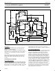
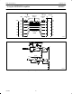
Figure 23 shows the VOX audio circuit example. A description of
its operation for voice activated transmission follows.
Audio generated by the electret microphone is fed into the
non-inverting input of preamp A1 and the signal amplified by 12dB.
The biasing is accomplished by the resistive divider which provides
a level of half the supply voltage which is connected through a 100k
resistor to the non-inverting terminal of A1. This automatically
provides ratiometric common mode biasing set at V
CC
/2 for the
device. This level is then transferred directly to the following
amplifier, A2, setting its DC operating point. The DC gain of both
stage A1 and A2 are unity so the cumulative DC error is not
multiplied by stage gain. The peak voice level is approximately
100mV
RMS
at the input to A1 from the microphone and this is
boosted to 400mV
RMS
. The feedback network gain has a low
frequency corner at 160Hz and is flat up to the intersection of the
closed loop gain with the open loop gain curve at nearly 500kHz.
This would increase the noise bandwidth to an excessive degree
unnecessary for voice channel communication. A band limiting
network is, therefore, inserted across the feedback resistor to limit
response to a nominal 5kHz.
Amplifier stage A2 is used to provide high level audio to the
rectifier-filter stage for the rapid generation of a DC control signal for
operating the voice activated switch function. Stage A2 gain is set
to 20dB in order to allow activation of the voice channel on the rising
edge of the first voice syllable. An attack time of 20ms is
implemented by adjusting the input charging impedance (R
S
)
between the rectifier and the A2 amplifier output. AC coupling must
be used to isolate the DC common-mode voltage of the amplifier
from the rectifier/storage capacitor and to allow only audio
frequencies to drive the switching circuit. Amplifier A3 provides a
high impedance unity gain buffer to allow a very slow decay rate to
be applied to the time constant capacitor, C
T
. The output of the
storage capacitor reaches approximately 3.2V for a 250ms duration
600Hz burst signal. Diode D1 (1N914) provides a negative clamp
action which forces the full peak-to-peak voltage from A2 to charge
the storage capacitor. D2 then acts to charge the capacitor to the
peak input voltage minus one diode drop, 0.7V. Finally, the buffered
DC control signal is fed to A4 which acts as a threshold comparator
with extremely high gain and controlled hysteresis. This provides a
positive going signal for releasing the NE578 from its inhibit mode
when voice input is present. The NE578 is switched from standby
mode when voice input is present. The NE578 is switched from
standby mode to the active state by raising the voltage on Pin 8 of
the device above 2V. Shutting the audio channel off requires this pin
to be driven below 100mV. This demands the extremely wide output
voltage swing of the NE5234 in order to reach this near to the
negative rail voltage. The voltage threshold of the comparator, A4,
is adjustable by use of the sensitivity control, R
S
. It is used to allow
the activation level to be raised or lowered depending upon the
ambient audio level in the transmitter vicinity.
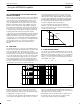
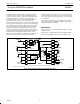
+3V
–
+
600Ω
a. VCVS Low Pass Filter
+
–
RR
R1
R4
C1
C1
R5
C2
C2
R2
R3
+5V
b. VCVS Band Pass Filter
R
i
R
f
R1
R2
–3V
V
OUT
V
OUT
V
IN
V
IN
SL00649
Figure 21. Active Filters
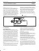
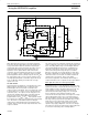
6kΩ
600Ω
10kΩ
10kΩ
2
3
1
6
5
7
9
10
8
13
12
14
–
+
AUDIO IN
LEFT
AUDIO IN
RIGHT
4
11
+
–
LEFT CHANNEL
OUT
RIGHT CHANNEL
OUT
NE/SA5234
#1
BRIDGE AMP #2
NE5234
–
+
–
+
–
+
+3V
PIN
X(–1)
–3V
SL00650
Figure 22. Stereo Bridge Amp