
Stereo Amplifier User Manual


Philips Semiconductors Application note
AN1651Using the NE/SA5234 amplifier
1991 Oct
3
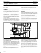
47k
47k
V
IN
V
OUT
V
CC
+
–
5V
CONVENTIONAL OP AMP PHILIPS NE5234
t
t
V
CC
V
OUT
V
OUT
V
IN
V
IN
V
GND
V
GND
V
GND
V
CC
5V
SL00569
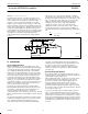
Figure 2. Output Inversion Protection
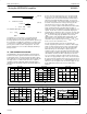
6
5
4
3
2
1
0.5
-1
-0.1
+0.1
“N-MODE”
CMRR
V
EE
+1 < V
CM
< V
CC
“LARGE
SIGNAL”
CMRR
“N-MODE”
CMRR
V
EE
< V
CM
< V
EE
+0.5V
V
EE
V
OS
mV
COMMON MODE VOLTAGE (VOLTS)
NE5234 Common-Mode Operating Regions
SL00631
Figure 3.
For negative going input signals, which drive the inputs toward the
V
EE
rail and below, another set of diode-connected transistors come
into operation. These steer the current from the input into Q8 or Q9
emitter circuits again preventing the reversal effect.
Figure 3 shows graphically how the N and P mode transitions relate
to the common-mode input voltage and the offset voltage V
OS
.
Intermediate Amplifier and Output Stage
(Figure 4)
The intermediate stage is isolated from the input amplifier by emitter
followers
to prevent any adverse loading effect. This stage adds gain to the
over all amplifier and translates levels for the following class-AB
current-control driver. Note that I
2
is the inverting input and I
1
the
non-inverting input. The output is taken from multiple collectors on
the non-inverting side and provides matching for the following stage.
Class-AB control of the output stage is achieved by Q61 and Q62
with the associated output current regulators. These act to monitor
the smallest current of the non-load supporting output transistor to
keep it in conduction. Thus, neither Q71 or Q81 is allowed to cutoff
but is forced to remain in the proper Class-AB region.
Overload protection is provided by monitor circuits consisting of
R76-D2 for sinking and R86-D3 for sourcing condition at the output.
When the output current, source or sink, reaches 15 milliamperes,
drive current to the stage is shunted away from current sources IB6
or IB9 reducing base current to driver transistors Q72 and Q82
respectively.
The prevention of saturation in the output stage is achieved by
saturation detectors Q78 and Q88. When either Q71 or Q81
approaches saturation, current is shunted away from the driver
transistors, Q72 or Q83 respectively.
III. CHARACTERISTICS
Internal Frequency Compensation
The use of nested Miller capacitors C2 through C6, in the
intermediate and output sections, provides the overall frequency
compensation for the amplifier. The dominant pole setting capacitor,
C2, provides a constant 6dB/octave roll-off to below the unity gain
frequency of 2.5MHz. Figure 5 shows the measured frequency
response plot for various values of closed-loop gains.