
Instructions

EN
UF20.241 Installation Manual
Product Description
The UF20.241 buffer module is a supplementary device for regulated DC power supplies and can be
used as power source to bridge failures of the DC voltage supply system or to extend the hold-up time
after loss of the AC power or to deliver short-term peak current above the current rating of the power
supply.
Intended Use
This device is designed for installation in an enclosure and is intended for commercial use, such as in
industrial control, process control, monitoring and measurement equipment or the like. Do not use this
device in equipment where malfunction may cause severe personal injury or threaten human life.
Installation Instructions
Install the device in an enclosure providing protection against electrical, mechanical and fire hazards.
Install the device onto a DIN-rail according to EN 60715 with the power terminals on the top of the
unit.
The device can be powered from a regulated power supply or a similar DC source. The voltage
between the supply voltage terminals and the PE terminal must not exceed 60Vdc continuously.
The device must be powered from a PELV or SELV source or an "Isolated Secondary Circuit" in order
to maintain a SELV or PELV level.
Use an appropriately sized 24V power supply, which can deliver the additional internal current
consumption, required to charge the capacitors.
Check for correct supply voltage polarity. The device will not operate when the voltage is reversed.
Make sure that the wiring is correct by following all local and national codes. Use appropriate copper
cables that are designed for a minimum operating temperature of 60°C for ambient temperatures up to
+45°C, 75°C for ambient temperatures up to +60°C and 90°C for ambient temperatures up to +70°C.
Ensure that all strands of a stranded wire enter the terminal connection.
The device is designed for pollution degree 2 areas in controlled environments.
No condensation or
frost is allowed.
The enclosure of the device provides a degree of protection of IP20.
The device is designed for convection cooling and does not require an external fan. Do not obstruct
airflow and do not cover ventilation grid!
Keep the following minimum installation clearances: 40mm on top, 20mm on the bottom, 0mm left and
right side.
The device is designed for altitudes up to 6000m (19685ft).
The maximum surrounding air temperature is +70°C (+158°F). The operational temperature is the
same as the ambient or surrounding air temperature and is defined 2cm below the device.
The device is designed to operate in areas between 5% and 95% relative humidity.
For EMI reasons, signal lines (ready, active and inhibit) must be shorter than 30m.
Functional Description
Green Status LED
This LED is on solid, when the capacitor is charged. During charging, the LED is flashing with a slow
frequency and rapid flashing is an indication of a buffer event.
Back-up Threshold Selector
The buffer behavior can be selected with the back-up jumper between “Fixed Mode” and “Variable
Mode”. In "Fixed Mode", the unit switches to buffer mode as soon as the voltage falls below 22.5V. In
"Variable Mode", the unit switches to buffer mode when input voltage decreases by 1V. Voltage
changes slower than 0.54V/s will be ignored if the voltage is above 22.5V. Below 22.5V buffering
starts immediately.
Inhibit Input
The inhibit input disables or stops buffering. Connect pin 6 to the positive pole of the supply voltage or
to an external control voltage and pin 9 to the corresponding negative pole. Inhibiting the unit also
discharges the internal capacitors. Charging of the capacitor is not possible when the buffer module is
in inhibit mode. The current of the inhibit input is limited to 4mA by the buffer module.
Active Signal
The signal “Active” (pin 7) is an opto-coupler output which is low ohmic while capacitors are
discharged. The maximal signal current between pin 6 and 7 is 10mA and the maximal voltage is 35V.
Ready Signal
The signal “Ready” (pin 8) is an opto-coupler output which is low ohmic when capacitors are fully
charged. The maximal signal current between pin 6 and 8 is 10mA and the maximal voltage is 35V.
Technical Data
All values are typical figures specified at 24Vdc supply voltage in standby
mode at 25°C ambient, no capacitor charging and after a 5 minutes run-in
time unless otherwise noted.
Supply voltage DC 24V -20%/+25%
Minimum input voltage to
start charging and to
enable buffer mode
23Vdc
Transfer voltage to switch
into buffer mode
22.5Vdc
V
IN
-1V
In fixed mode
In variable mode
Internal current
consumption
max. 0.6A Includes charging
current
Current limitation in buffer
mode
21.5A
Buffer time min. 220ms At 22.5V, 20A
min. 430ms At 22.5V, 10A
typ. 310ms At 22.5V, 20A
typ. 670ms At 22.5V, 10A
typ. 43s At 22.5V, 0.1A
Charging time 25s For initial charging
18s For recharging shortly
after a buffer event
Power losses 1.9W
Temperature range -25°C to +70°C
Max. wire size (litz wire) 4mm² For power terminals
Wire size AWG AWG 20-10 For power terminals
Max. wire diameter 2.8mm For power terminals
Wire stripping length 10mm/ 0.4inch For power terminals
Max. wire size (litz wire) 2.5mm² For signal terminals
Wire size AWG AWG 22-14 For signal terminals
Max. wire diameter 2.25mm For signal terminals
Wire stripping length 6mm/ 0.25inch For signal terminals
Tightening torque 0.4Nm/ 3.5lb.inch For signal terminals
Size (wxhxd) 62x124x102mm Without DIN-rail
Weight 740g / 1.63lb
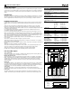
Functional Diagram
Supply
Voltage
Status
LED
Inhibit
Controller
(7)
(6)
Reverse
Polarity
Protection
Safety and
Overvoltage
Protection
Boost
Converter
Charger
Safety
Circuits
and
Discharge
Circuit
Storrage
Capacitor
Chassis
Ground
-
-
+
+
Voltage
Monitor
(9)
(8)
+
Ready
Active
Back-up
Level
Selector
Wiring Scheme
Signals
Input
Buffer
Module
Load
Power
Supply
Output
Input
+
-
+
-
+
-
L N
PE
Signals
Input
Buffer
Module
+
-
Signals
Input
Buffer
Module
+
-
Buffer modules can be connected in parallel to increase the output
ampacity or the hold-up time.
LED Signal Pattern
Ready
Charging
Buffering
Green Status LED: