
Owner's manual
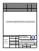
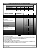

ºC/W50
θ
jc
Package thermal resistance
ºC/seconds250/10Lead solder temperature/time
ºC150-65TstgStorage temperature
ºC125-55T
C
Operating temperature
Volts70V
CC
Supply voltage
UnitsMaxMinSymbolParameter
TABLE II. MAXIMUM RATINGS
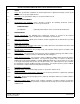
ms10STARTUP TIME
ppm±10
70 °C ± 3 °CFREQUENCY AGING (AFTER 1 YEAR)
ppm±1.5
70 °C ± 3 °CFREQUENCY AGING (AFTER 30 DAYS)
%60/40 or betterDUTY CYCLE
6/nS2.5
> 125 MHZ
6/nS3
> 70 MHZ - 125 MHZ
6/nS5
Up to 70 MHZ
Output frequency:
RISE / FALL TIME
@ worst case, Vcc = 3.0, T = 125 °C
N/ASquarewaveOUTPUT WAVEFORM
5/Vdc
V
CC
x 0.9OUTPUT VOLTAGE - LOGIC "1"
5/VdcV
CC
x 0.1OUTPUT VOLTAGE - LOGIC "0"
6/-
CMOSLOAD
mA30100 MHZ - 150 MHZ
mA2060 MHZ - 99.99 MHZ
mA1512 MHZ - 59.99 MHZ
mA12Less than 12 MHZ
Out
p
ut fre
q
uenc
y
:
INPUT CURRENT
Measured without load at 3.63 Vdc
Vdc3.63.33SUPPLY VOLTAGE
1/, 4/
See Table IFREQUENCY/TEMPERATURE STABILITY
MHz1500.75FREQUENCY RANGE
UNITSMAX.NOM.MIN.
NOTESLIMITS
TEST CONDITIONS 2/, 3/ELECTRICAL PARAMETER
TABLE Ill. ELECTRICAL PERFORMANCE CHARACTERISTICS
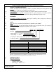
NOTES
1. The limit for frequency/temperature stability (tolerance) shall be referenced to the specified nominal output frequency, except
for temp code H as noted above.
2. Unless otherwise specified, the limits are over the full operating temperature range and under specified load conditions.
3. Unless otherwise specified, all measurements are in accordance with MIL-PRF-55310.
4. Up to 30 days after shipment.
5. Voltage values are with respect to network ground terminal.
6. A standard CMOS load of 10 kOhm || 15 pF shall be used, except for frequencies greater than 125 MHZ, where the load
shall be 5 pF. See MIL-PRF-55310/26 for CMOS waveform measurement definitions.
THIS DOCUMENT IS CONSIDERED PROPRIETARY TO Q-TECH CORPORATION
DO NOT COPY OR DISTRIBUTE WITHOUT Q-TECH CORPORATION APPROVAL
Q-Tech Corporation
10150 W. Jefferson Blvd.
Culver City, CA. 90232
Specification number: QT625L rev. F
Sheet 4 of 5