
User's Manual PCMCIA Asynchronous Adapter MPAP-100

18 Receive FIFO Timeout Register
The Receive FIFO Timeout Register is used to control the operation of the external
receive FIFO timeout feature. The address of this register is Base+D (hex). This register can be
ignored if the external FIFOs are not being used. See page 38 for details on the receive FIFO
timeout feature.
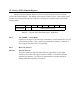
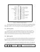
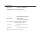
timeout interval (0-63)0X16_MODE
Bit 0Bit 1Bit 2Bit 3Bit 4Bit 5Bit 6Bit 7
Table 16 --- Receive FIFO Timeout Register - Read/Write
Bit 7: X16_MODE --- Clock Mode:
If this bit is set (logic 1), the data clock is divided by 16 (prescaled) before it is fed
to the timeout circuitry. This is useful for asynchronous operation. If this bit is
clear (logic 0), the data clock is not prescaled.
Bit 6: Reserved, always 0.
Bits 5-0: Timeout Interval:
This is the number of character-times that must elapse before a non-empty
external receive FIFO will trigger a timeout condition. This interval assumes
eight bits per character, so it will be an approximation for modes running at
settings other than eight bits per character.