MPA-100 RS-232 SYNCHRONOUS ADAPTER CARD User's Manual INTERFACE CARDS FOR IBM PC/AT AND PS/2 QUATECH, INC. 5675 Hudson Industrial Parkway Hudson, Ohio 44236 TEL: (330) 665-9000 FAX: (330) 665-9010 http://www.quatech.
Warranty Information Quatech Inc. warrants the MPA-100 to be free of defects for one (1) year from the date of purchase. Quatech Inc. will repair or replace any adapter that fails to perform under normal operating conditions and in accordance with the procedures outlined in this document during the warranty period. Any damage that results from improper installation, operation, or general misuse voids all warranty rights.
The information contained in this document cannot be reproduced in any form without the written consent of Quatech, Inc. Likewise, any software programs that might accompany this document can be used only in accordance with any license agreement(s) between the purchaser and Quatech, Inc. Quatech, Inc. reserves the right to change this documentation or the product to which it refers at any time and without notice.
Table of Contents 1. INTRODUCTION . . . . . . . . . . . . . . . . . . . . . . . . . . . . . . . . . . . . . . . . . . . . . . . . 1-1 2. HARDWARE INSTALLATION . . . . . . . . . . . . . . . . . . . . . . . . . . . . . . . . . . . 2-1 3. ADDRESSING . . . . . . . . . . . . . . . . . . . . . . . . . . . . . . . . . . . . . . . . . . . . . . . . . . . . 3-1 4. INTERRUPTS . . . . . . . . . . . . . . . . . . . . . . . . . . . . . . . . . . . . . . . . . . . . . . . . . . . . 4-1 4.
MPA-100 User's Manual iv
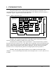
1. INTRODUCTION The Quatech MPA-100 is a single channel, synchronous RS-232 compatible serial communication port for systems utilizing the architecture of the IBM AT personal computer or compatible. Figure 1 depicts the layout of the MPA-100. Figure 1 MPA-100 Board Layout Quatech, Inc.
MPA-100 User's Manual 1-2
2. HARDWARE INSTALLATION If the default address and interrupt settings are sufficient, the MPA-100 can be quickly installed and put to use. The factory default settings are listed below in Table 1. Table 1 Default Resource Settings Address Interrupt 300 hex IRQ 5 TxDMA DMA/DRQ 3 RxDMA DMA/DRQ 1 1. If the default settings are correct, skip to step 2, otherwise refer to chapters 3, 4, and 7 for detailed information on how to set the address, IRQ, and DMA levels. 2.
MPA-100 User's Manual 2-2
3. ADDRESSING The MPA-100 occupies a continuous 8 byte block of I/O addresses. For example, if the base address is set to 300H, then the MPA-100 will occupy address locations 300H-307H. The base address of the MPA-100 may be set to any of the first 64 Kbytes (0 - FFFFH) of available I/O address space through the settings of dip switches SW1 and SW2. SW1 allows the user to select the higher address signals A15 - A8. SW2 allows the user to select the lower address signals A7 - A3.
The first four bytes, Base+0 through Base+3, of address space on the MPA-100 contain the internal registers of the SCC. The next two locations Base+4 and Base+5 contain the Communications Register and the Configuration Register. The last two address port locations are reserved for future use. The entire address range of the MPA-100 is shown in Table 2.
4. INTERRUPTS The MPA-100 supports eleven interrupt levels: IRQ2 -7, IRQ10 - 12, and IRQ14 - 15, and selects which interrupt level is in use through jumper packs J5 and J6. The MPA-100 has three interrupt sources: interrupt on terminal count, interrupt on test mode, and interrupt from the SCC. The interrupt source is selected by bits D4 and D5 of the Configuration Register, see Section 8 for details.
4.1 Using Terminal Count to Generate Interrupts The MPA-100 allows the option of generating an interrupt whenever the Terminal Count (TC) signal is asserted. Terminal Count is an indicator generated by the system’s DMA controller, which signals that the number of transfers programed into the DMA controller’s transfer register have occurred. This board feature only works when the interrupt sharing feature is selected on jumper J4.
5. JUMPER CONFIGURATIONS The MPA-100 utilizes various jumper blocks which allow the user to customize their hardware configuration. The following sections explain the function and setting of each of the jumper blocks on the MPA-100. 5.1 DTE/DCE Configuration - J2, J11, & J12 The jumper packs J2, J11, and J12 control the DTE/DCE configuration of the MPA-100. J2 determines the board setting (DTE or DCE) while the jumper packs J11 and J12 control the routing of the signals to the DB-25 connector.
5.3 Interrupt Level Selection - J5 & J6 Jumper blocks J5 and J6 select the interrupt level that the MPA-100 utilizes. Interrupt levels IRQ2 - IRQ7 reside on J5, while interrupt levels IRQ10 - IRQ12 and IRQ14 - IRQ15 reside on J6. Table 5 and Table 6 summarize the jumper block selections for J5 and J6. The IRQ levels are also marked on the MPA-100 silkscreen for easy identification. Table 5 Jumper block J5 selections.
5.4 Transmit DMA Selection - J8 J8 Selects the DMA channel to be used for Transmit DMA. Three channels (1 - 3) are available on the MPA-100 for DMA. When selecting a DMA channel, both the DMA acknowledge (DACK) and the DMA request (DRQ) for the appropriate channel need to be selected. Table 7 summarizes the jumper block selections for J8. Table 7 Jumper block J8 selections. DMA Channel Pins Channel 1 1-7 2-8 Channel 2 3-9 4-10 Channel 3 (Default) 5-11 6-12 5.
NOTE: Since it is illegal to perform DMA on transmit and receive on the same DMA channel, jumper blocks J7 and J8 should never have the same pins connected. This could result in damage to the system. 5.6 SYNCA to RLEN Control - J7 J7 controls the signal path from the RLEN bit in the Communications Register to the SYNCA input to the SCC. If J7 is installed and the SCC is in external SYNC mode, setting the RLEN bit high will assert the SYNCA pin.
6. SCC GENERAL INFORMATION The Serial Communications Controller (SCC) is a dual channel, multi-protocol data communications peripheral. The MPA-100 provides a single channel for communications, however, to provide full DMA capabilities with complete modem control line support, both channels of the SCC can be utilized. The SCC can be software configured to satisfy a wide variety of serial communications applications.
6.1 Accessing the Registers The mode of communication desired is established and monitored through the bit values of the internal read and write registers. The register set of the SCC includes 16 write registers and 9 read registers. These registers only occupy four address locations, which start at the MPA-100's physical base address that is configured via the on board switches. This and all other addresses are referenced from this base address in the form Base + Offset.
Example 2: Monitoring the status of the transmit and receive buffers in RR0 of Channel A. Register 0 is addressed by default if no register number is written to WR0 first. mov add in Example 3: dx,base dx,ContA ax,dx Write data into the transmit buffer of channel A. mov out Example 4: ; load base address ; add control reg A offset (1) ; read the status dx,base dx,al ; load base address ; write data in ax to buffer Read data from the receive buffer of channel A.
and receive clocks. These clocks can be programmed in WR11 to come from the RTXC pin, the TRXC pin, the output of the BRG, or the transmit output of the DPLL. Programming of the clocks should be done before enabling the receiver, transmitter, BRG, or DPLL. Table 11 SCC write register description.
6.2 Baud Rate Generator Programming The baud rate generator (hereafter referred to as the BRG) of the SCC consists of a 16-bit down counter, two 8-bit time constant registers, and an output divide-by-two. The time constant for the BRG is programmed into WR12 (least significant byte) and WR13 (most significant byte).
6.3 SCC Data Encoding Methods The SCC provides four different data encoding methods, selected by bits D6 and D5 in WR10. These four include NRZ, NRZI, FM1 and FM0. The SCC also features a digital phase-locked loop (DPLL) that can be programmed to operate in NRZI or FM modes. Also, the SCC contains two features for diagnostic purposes, controlled by bits in WR14. They are local loopback and auto echo.
7. DIRECT MEMORY ACCESS Direct Memory Access (DMA) is a way of transferring data on the ISA bus directly to and from memory, resulting in high data transfer rates with very low CPU overhead. The ISA bus DMA channel(s) to be used are selected through jumper packs J6 and J7. The sources for these requests originate from the SCC and can be programmed for a variety of DMA modes. These modes include DMA request on transmit, DMA request on receive, and DMA request on both transmit and receive.
When using the channel A DTR/REQ pin for transmit DMA the SCC must be programmed so that the request release timing of this pin is identical to the WAIT/REQ timing. This is done by setting bit D4 of write register 7 prime. NOTE: Even though the W/REQA pin can be used for both DMA transmit and DMA receive, obviously it cannot be used for both simultaneously. Therefore, bits D0 and D1 of the Configuration Register should never be cleared at the same time while bits D2 and D3 are both set.
8. CONFIGURATION REGISTER The MPA-100 is equipped with an onboard register used for configuring information such as DMA enables, DMA sources, interrupt enables, and interrupt sources. Below is a detailed description of the Configuration Register. The address of this register is Base+5. Table 13 details the bit definitions of the Configuration Register. Table 13 Configuration Register - Read/Write D7 D6 D5 D4 0 0 INTS1 D3 D2 D1 D0 INTS0 DMREN DMTEN RXSRC TXSRC D7-D6 - Reserved, always 0.
D1 -RXSRC, RECEIVE DMA SOURCE: When set (logic 1), this bit allows the source for Receive DMA to come from the W/REQB pin of channel B on the SCC. When cleared (logic 0), the source for Receive DMA comes from the W/REQA pin of channel A on the SCC. D0 -TXSRC, TRANSMIT DMA SOURCE: When set (logic 1), this bit allows the source for Transmit DMA to come from the DTR/REQA pin of channel A on the SCC. When cleared (logic 0), the source for Transmit DMA comes from the W/REQA pin of channel A of the SCC.
9. COMMUNICATIONS REGISTER The MPA-100 is equipped with an onboard Communications Register which gives the user options pertaining to the clocks and testing. The user can specify the source and type of clock to be transmitted or received. Test mode bits pertain only to the DTE versions and can be ignored if using a DCE configured MPA-100. The address of this register is Base+4. Table 15 and the descriptions that follow detail the Communications Register.
D4 -REMOTE LOOPBACK ENABLE: When set (logic 1), this bit allows the DTE to test the transmission path up to and through the remote DCE to the DTE interface and the similar return transmission path. When cleared (logic 0), no testing occurs. If jumper J7 is in place the Remote Loopback is also used to control the Sync input of the Channel A data receiver. This is useful in situations where it is desired to receive unformatted serial data.
10. DTE/DCE CONFIGURATION As indicated earlier in this manual, the MPA-100 can be configured as either a Data Terminal Equipment (DTE) or a Data Communications Equipment (DCE) device. The differences between these configurations include signal definitions, connector pin out, and clocking options. In order to simplify matters, an in depth description of each configuration is provided in the next two sections.
10.1 DTE Configuration The MPA-100 is configured as a DTE device by correctly setting jumper packs J2, J11 and J12. See Section 5, Table 3 for this configuration information. The control signals the DTE can generate are Request To Send (RTS) and Data Terminal Ready (DTR). It can receive the signals Carrier Detect (CD), Clear To Send (CTS), and Data Set Ready (DSR).
The testing signals the DTE can generate are the Local Loopback Test (LL) and the Remote Loopback Test (RL). These signals are generated from the onboard Communications Register. When a Test Mode (TM) condition is received, an interrupt can be generated on the DTE. Table 16 summarizes the signals on the DTE.
Control signals the DCE can generate are the Clear to Send (CTS), Carrier Detect (CD), and Data Set Ready (DSR). It can receive the signals Data Terminal Ready (DTR) and Ready to Send (RTS). All the control signals are handled through channel A of the SCC, with the exception of the CD signal, which is generated on the DTR/REQB pin (pin 24) of the SCC.
Table 17 DCE Signals Signal Received RTS X CTS DTR Generated SCC Pin or Register Bit CTSA pin of SCC X X RTSA pin of SCC DCDA of SCC DSR X DTR/REQA pin of SCC CD X DTR/REQB pin of SCC TxCLK X TRXCA pin of SCC X RTXC/TRXCB pin of SCC LL X Bit D5 of Comm.
MPA-100 User's Manual 10-6
11. EXTERNAL CONNECTIONS The MPA-100 is designed to meet the RS-232 standard through a D-25 connector. The MPA-100 uses a D-25 short body male connector (labeled CN1) for both the DTE and DCE configurations. Jumper blocks J2, J11, and J12 configure the connector pin out. Table 18 and Table 19 display the pin out definitions for both configurations while Figure 6 and Figure 7 illustrate the pin-outs for each of the configurations.
Table 19 DCE Connector Pin Definitions PIN SIGNAL RECEIVED GENERATED SOURCE 1 CGND 2 TXD X RXDA on SCC 3 RXD X TXDA on SCC 4 RTS X CTSA on SCC 5 CTS X RTSA on SCC 6 DSR X DTR/REQA on SCC 7 DGND 8 CD X DTR/REQB on SCC 9 N/C 10 N/C 11 RXCLK (DTE) N/A N/A N/A 12 N/C 13 N/C 14 N/C 15 TXCLK (DCE) X TRXCA on SCC 16 N/C 17 RXCLK (DCE) X RTXC pins on SCC 18 LL X D5 of COMM REG 19 N/C 20 DTR X DCDB on SCC 21 RL X D4 of COMM REG 22 N/C 23 N/C 24 TXCLK (DTE) X RTXC pins on SCC 25 TEST MODE X D7 of COMM REG MPA-100 Us
Figure 6 MPA-100 DTE Output Connector Configuration N/C N/C RxCLK (DTE) N/C N/C CD DGND DSR CTS RTS RxD TxD CGND 13 12 11 10 9 8 7 6 5 4 3 2 1 25 24 23 22 21 20 19 18 17 16 15 14 Test Mode (Output) TxCLK (DTE) N/C N/C RLBK (Output) DTR N/C LLBK (Output) RxCLK (DCE) N/C TxCLK (DCE) N/C Figure 7 MPA-100 DCE Output Connector Configuration CGND RxD TxD CTS 1 2 3 4 RTS 5 DTR 6 DGND 7 CD 8 N/C 9 N/C 10 RxCLK (DTE) 11 N/C 12 N/C 13 MPA-100 User's Manual 14 15 16 17 18 19 20 21 22 23 24 25 N/C TxCLK (DCE)
MPA-100 User's Manual 11-4
12. DEFINITION OF INTERFACE SIGNALS CIRCUIT AB - Signal Ground CONNECTOR NOTATION: DGND DIRECTION: Not applicable This conductor directly connects the DTE circuit ground to the DCE circuit ground. CIRCUIT CC - DCE Ready (Data Set Ready) CONNECTOR NOTATION: DSR DIRECTION: From DCE This signal indicates the status of the local DCE by reporting to the DTE device that a communication channel has been established.
CIRCUIT DD -Receiver Signal Element Timing(RxClk - DCE Source) CONNECTOR NOTATION: RXCLK (DCE) DIRECTION: From DCE This signal, generated by the DCE, provides the DTE with element timing information pertaining to the data transmitted by the DCE. The DTE can use this information for its received data.
CIRCUIT RL - Remote Loopback CONNECTOR NOTATION: RLBK DIRECTION: To DCE This signal provides a means whereby a DTE or a facility test center may check the transmission path up to and through the remote DCE to the DTE interface and the similar return transmission path. CIRCUIT TM - Test Mode CONNECTOR NOTATION: TEST MODE DIRECTION: From DCE This signal indicates to the DTE that the DCE is in a test condition.
MPA-100 User's Manual 12-4
13. SPECIFICATIONS Bus interface: IBM AT 16-bit bus Controller: Serial Communications Controller, 10 MHz (determined by user, typically an AMD 85C30). Interface: DTE: male D-25 connector Transmit drivers: RS-232: MC1488 or compatible Receive buffers: RS-232: MC1489 or compatible I/O Address range: 0000H - FFFFH Interrupt levels: IRQ 2-7, 10-12, 14-15 DMA levels: DMA Channel 1, 2, and 3 on transmit and receive. Physical Dimensions: 4.2” x 7.
MPA-100 User's Manual Version 4.12 March 2004 Part No.