MPAC-100 RS-232 PCI SYNCHRONOUS ADAPTER for PCI Card Standard compatible machines User's Manual QUATECH, INC. 662 Wolf Ledges Parkway Akron, Ohio 44311 TEL: (330) 434-3154 FAX: (330) 434-1409 www.quatech.
WARRANTY INFORMATION Quatech Inc. warrants the MPAC-100 to be free of defects for one (1) year from the date of purchase. Quatech Inc. will repair or replace any board that fails to perform under normal operating conditions and in accordance with the procedures outlined in this document during the warranty period. Any damage that results from improper installation, operation, or general misuse voids all warranty rights.
Copyright 2000 Quatech, Inc. NOTICE The information contained in this document is protected by copyright, and cannot be reproduced in any form without the written consent of Quatech, Inc. Likewise, any software programs that might accompany this document are protected by copyright and can be used only in accordance with any license agreement(s) between the purchaser and Quatech, Inc. Quatech, Inc.
Table of Contents 1 Introduction . . . . . . . . . . . . . . . . . . . . . . . . . . . . . . . . . . . . . . . . . . . . . . . . . . . . . . 7 1.1 System Requirements . . . . . . . . . . . . . . . . . . . . . . . . . . . . . . . . . . . . . . . . . 7 2 Hardware Installation . . . . . . . . . . . . . . . . . . . . . . . . . . . . . . . . . . . . . . . . . . . . 8 3 Windows 95/98 Installation . . . . . . . . . . . . . . . . . . . . . . . . . . . . . . . . . . . . . . 9 4 Other Operating Systems . . . . . . .
Table of Contents 15 Receive Pattern Character Register . . . . . . . . . . . . . . . . . . . . . . . . . . . . 16 Receive Pattern Count Register . . . . . . . . . . . . . . . . . . . . . . . . . . . . . . . . 17 Receive FIFO Timeout Register . . . . . . . . . . . . . . . . . . . . . . . . . . . . . . . . 18 External Connections . . . . . . . . . . . . . . . . . . . . . . . . . . . . . . . . . . . . . . . . . . . 18.1 5V fuse (pin 9) . . . . . . . . . . . . . . . . . . . . . . . . . . . . . . . . . . . . .
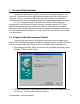
1 Introduction The Quatech MPAC-100 is a PCI Type card and is PCI PC Card Standard Specification compliant. It provides a single-channel RS-232 synchronous communication port. The base address and IRQ are configured through the PCI hardware and software using utility programs provided by Quatech. There are no switches or jumpers to set. The MPAC-100 uses a Zilog 85230-compatible Serial Communications Controller (SCC).
2 Hardware Installation Hardware installation for the MPAC-100 is a very simple process: 1. Turn off the power of the computer system in which the MPAC-100 is to be installed. 2. Remove the system cover according to the instructions provided by the computer manufacturer. 3. Install the MPAC-100 in any empty PCI expansion slot. The board should be secured by installing the Option Retaining Bracket (ORB) screw. 4. Replace the system cover according to the instructions provided by the computer manufacturer.
3 Windows 95/98 Installation Windows 95/98 maintains a registry of all known hardware installed in your computer. Inside this hardware registry Windows keeps track of all of your system resources, such as I/O locations, IRQ levels, and DMA channels. The "Add New Hardware Wizard" utility was designed to add new hardware and update this registry. An "INF" configuration file is included with the MPAC-100 to allow easy configuration in the Windows 95/98 environment.
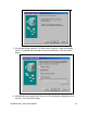
3. On the next dialog, select the "CD-ROM drive" checkbox. Insert the Quatech COM CD (shipped with the card) into the CD-ROM drive. Click the "Next" button. 4. Windows should locate the INF file on the CD and display a dialog that looks like this. Click the "Next" button.
5. Windows will copy the INF file from the CD and display a final dialog indicating that the process is complete. Click the "Finish" button.
3.2 Viewing Resources with Device Manager The following instructions provide step-by-step instructions on viewing resources used by the MPAC-100 in Windows 95/98 using the "Device Manager" utility. 1. Double click the "System" icon inside the Control Panel folder. This opens up the System Properties box. 2. Click the "Device Manager" tab located along the top of the System Properties box. 3. Double click the device group "Synchronous_Communication".
5. Click the "Resources" tab located along the top of the properties box to view the resources Windows has allocated for the MPAC-100 match the hardware configuration. Click "Cancel" to exit without making changes. 6. If changes to the automatic configuration are necessary for compatibility with existing programs, uncheck the "Use Automatic Settings" box and double-click on the Resource Type that needs to be changed.
4 Other Operating Systems Device drivers for Windows NT and OS/2 are also available for the MPAC-100. The board can be used under DOS and other operating systems as well in many circumstances. The software described below can be downloaded from the Quatech web site if it did not come with the board. 4.1 Windows NT The Windows NT device driver is installed by running the SETUP program. Up to 256 serial ports are supported.
Quatech's "QTPCI" utility supplies the information required when modifying the serial port settings of the application. This program should be run from real DOS, not in a Windows DOS box. Figure 13 shows the Basic Mode display for the MPAC-100 after the "Q" key has been pressed. In this example, the MPAC-100 uses I/O base address FF80 hex and IRQ 11. The hardware revision of the MPAC-100 is also displayed.
The QTPCI program is capable only of displaying the PCI configuration. It cannot be used to make changes. Quatech PCI Configuration Information Display Software Version 1.03 INSTRUCTIONS: -----------------------Press keys listed in the menu at the bottom of the screen. This program only displays information. It cannot make changes. Numbers preceeded by "0x" are hexadecimal. PCI BIOS detected, version 2.
and I/O regions, etc. Pressing the "N" key will show similar information for all non-Quatech PCI devices in the system, including those devices integrated on the motherboard. In this example, the "Base addr 0" resource is reserved. For users interested in even more details, PCI BIOS information can be displayed by pressing the "B" key. Pressing the "I" key displays the PCI interrupt routing table. Quatech PCI Configuration Information Display Software Version 1.
5 Using the MPAC-100 with Syncdrive Syncdrive is a synchronous communications software driver package designed to aid users of Quatech synchronous communication hardware in the development of their application software. Syncdrive is included free of charge with all Quatech MPA-series synchronous communication products. The MPAC-100 is backward-compatible with software written for Quatech ISA-bus synchronous adapters and it operates with Syncdrive.
6 Addressing The MPAC-100 occupies a continuous 16-byte block of I/O addresses. For example, if the base address is set to 300 hex, then the MPAC-100 will occupy address locations 300 hex to 30F hex. If the computer in which the MPAC-100 is installed is running PCI Card and Socket Services, the base address is set by the client driver. If PCI Card and Socket Services are not being used, the base address is set by the MPAC-100 enabler program.
7 Interrupts The MPAC-100 will operate using the interrupt level (IRQ) assigned by the PCI system. Interrupts can come from the SCC, the internal FIFOs or RS-232 test mode. The interrupt source is selected by bits 4 and 5 of the Configuration Register (see page 41). When using interrupts with the MPAC-100, the application must have an interrupt service routine (ISR). There are several things that an ISR must do to allow proper system operation: 1.
8 SCC General Information The Serial Communications Controller (SCC) is a dual channel, multi-protocol data communications peripheral. The MPAC-100 provides a single channel for communications, however, portions of the second channel can be utilized to support some special circumstances. The SCC can be configured to satisfy a wide variety of serial communications applications.
8.1 Accessing the registers The mode of communication desired is established and monitored through the bit values of the internal read and write registers. The register set of the SCC includes 16 write registers and 9 read registers. These registers only occupy four address locations, which start at the MPAC-100's physical base address that is configured via the on board switches. This and all other addresses are referenced from this base address in the form Base+Offset.
Example 3: Write data into the transmit buffer of channel A. mov out Example 4: dx, base dx, al ; load base address ; write data in ax to buffer Read data from the receive buffer of channel A.
for its clock-on-receive. Programming of the clocks should be done before enabling the receiver, transmitter, BRG, or DPLL.
8.2 Baud Rate Generator Programming The baud rate generator (hereafter referred to as the BRG) of the SCC consists of a 16-bit down counter, two 8-bit time constant registers, and an output divide-by-two. The time constant for the BRG is programmed into WR12 (least significant byte) and WR13 (most significant byte).
8.4 Support for SCC Channel B The MPAC-100 is a single-channel device. Portions of SCC channel B are used to augment channel A. Channel B cannot be used for transmit, but may be used for receive, subject to certain limitations. 8.4.1 Receive data and clock signals The receive data signals RXDA and RXDB are tied together. The receive clock input signals RTxCA and RTxCB are also tied together. This can be useful in unusual applications.
8.5 SCC Incompatibility Warnings Due to the SCC implementation used by the MPAC-100, there are two minor incompatibilities that the software programmer must avoid. 8.5.1 Register Pointer Bits In a Zilog 85230, the control port register pointer bits can be set in either channel. With the implementation on the MPAC-100, however, both parts of an SCC control port access must use the same I/O address.
9 FIFO Operation The MPAC-100 is equipped with 1024-byte internal FIFOs in the transmit and receive data paths. These FIFOs are implemented as extensions of the SCC's small internal FIFOs. They have been designed to be as transparent as possible to the software operating the MPAC-100. By using these FIFOs, it is possible to achieve high data rates despite the MPAC-100 not supporting DMA. The FIFOs are disabled by default after card insertion, power-up, or a system reset. 9.
9.2.2 Receive FIFO The receive FIFO can service the receiver of either channel A or channel B of the SCC. If RXSRC (bit 1) of the Configuration Register (see page 41) is logic 1, the receive FIFO will service SCC channel B. If RXSRC is logic 0, the receive FIFO will service SCC channel A. If the FIFOs are enabled, an I/O read from either SCC Data Port (channel A or channel B) will read a byte from the receive FIFO.
9.3.1 Using channel A for both transmit and receive This is the mode in which most applications will run. Set RXSRC (bit 1) in the Configuration Register to logic 0. This will configure the MPAC-100 to use W/REQA for receive DMA and DTR/REQA for transmit DMA. In addition to any other desired SCC configuration, ensure that the following bits are set according to Table 6: Registe r Bit(s) Value Function Enable DMA request on W/REQA. This bit should be set after the other bits in WR1 are set as desired.
9.3.2 Using channel B for receive The MPAC-100 supplies only limited support for SCC channel B. This mode, therefore, is not recommended for most applications. Set RXSRC (bit 1) in the Configuration Register to logic 1. This will configure the MPAC-100 to use W/REQA for transmit DMA and W/REQB for receive DMA. In addition to any other desired SCC configuration, ensure that the following bits are set according to Table 7: Register Bit(s) 7 WR1A 6 5 1 Value Function Enable DMA request on W/REQA.
9.4 FIFO status and control Several registers are used to control the FIFOs and monitor their status. These registers are detailed in other chapters of this manual. 9.4.1 Interrupt status Three interrupt statuses, listed in Table 8, can be generated by four events related to FIFO activity. In each case, a latched bit in the Interrupt Status Register is set to a logic 1 (see page 43). These bits are write-clear, meaning that software must write a 1 to a bit in order to clear it.
IMPORTANT Software can differentiate between the two types of RX_FIFO interrupts by examining the RXH bit in the FIFO Status Register. If RXH is clear (logic 0), the interrupt occurred because of a timeout. 9.4.2 Resetting the FIFOs The FIFOs are automatically disabled and reset at powerup or when the MPAC-100 is inserted into a PCI socket. The transmit and receive FIFOs can also be independently reset by setting and clearing the appropriate bits in the FIFO Control Register.
9.6 Receive pattern detection The internal FIFOs are most useful in bit-synchronous operational modes because the SCC can generate a Special Condition interrupt when the closing flag of a bit-synchronous frame is received. This allows the SCC to run with per-character receive interrupts disabled while DMA transfers occur between the SCC and internal FIFOs. Byte-synchronous modes such as bisync, however, do not benefit from such a hardware assist for detecting the end-of-frame condition.
9.7 Receive FIFO timeout With asynchronous operational modes, the same problem exists. Namely, how is one to determine when a reception is complete? While the receive pattern detection may be useful here, the MPAC-100 also offers a timeout feature on the internal receive FIFO.
10 Communications Register The Communications Register is used to set options pertaining to the clocks. The source and type of clock to be transmitted or received can be specified. External synchronization and RS-232 DTE test modes and can also be controlled with this register. The address of the Communications Register is Base+4. Table 9 details its bit definitions.
SW_SYNC ('C' option is used) This bit is used to drive the active-low SYNC input of the channel A receiver. The SYNC signal is asserted when this bit is set (logic 1), and is deasserted when this bit is clear (logic 0). This is useful in situations where it is necessary to receive unformatted serial data, as it allows the SCC receiver to be manually placed into sync under program control. This bit is ignored if bit 6 is set (logic 1).
11 Configuration Register The Configuration Register is used to set the interrupt source and enable the interface between the SCC and the internal FIFOs. The address of this register is Base+5. Table 10 details the bit definitions of the register. Bit 7 Bit 6 Bit 5 Bit 4 Bit 3 1 0 INTS1 INTS0 0 Bit 2 Bit 1 FIFOEN RXSRC Bit 0 0 Table 10 --- Configuration Register - Read/Write Bit 7: Internal Data FIFOs Present --- Reserved, always 1.
Bit 1: RXSRC --- Receive FIFO DMA Source: This bit determines which SCC pins are used to control transmit and receive DMA transactions between the SCC and the internal FIFOs (when enabled). The transmit data FIFO is always used with SCC channel A. The receive data FIFO may be used with SCC channel A by setting RXSRC to logic 0, or with SCC channel B by setting RXSRC to logic 1. (See page 29 for information on using channel B.
12 Interrupt Status Register The Interrupt Status Register is used to determine the cause of an interrupt generated by the MPAC-100. The address of this register is Base+8. Table 11 details the bit definitions of the register. The interrupt source in the Configuration Register (see page 41) must be set to INTSCC for any of the statuses indicated by this register to occur. This register can be ignored if the internal FIFOs are not being used.
13 FIFO Status Register The FIFO Status Register is used to return current status information about the internal FIFOs. The address of this read-only register is Base+9. Table 12 details the bit definitions of the register. This register can be ignored if the internal FIFOs are not being used. Bit 7 Bit 6 Bit 5 Bit 4 Bit 3 Bit 2 Bit 1 Bit 0 0 RXF RXH RXE 0 TXF TXH TXE Table 12 --- FIFO Status Register - Read Only Bit 7: Reserved, always 0.
14 FIFO Control Register The FIFO Control Register is used to control the internal data FIFOs. The address of this register is Base+A (hex). Table 13 details the bit definitions of the register. This register can be ignored if the internal FIFOs are not being used. Bit 7 Bit 6 0 EN_PAT Bit 5 Bit 4 EN_TO RX_RESET Bit 3 Bit 2 Bit 1 Bit 0 0 0 0 TX_RESET Table 13 --- FIFO Control Register - Read/Write Bit 7: Reserved, always 0.
15 Receive Pattern Character Register The Receive Pattern Character Register is used to set the character value to be used in receive pattern detection. The address of this register is Base+B (hex). This register can be ignored if the internal FIFOs are not being used. Bit 7 Bit 6 Bit 5 Bit 4 Bit 3 Bit 2 Bit 1 Bit 0 character value (0-255) Table 14 --- Receive Pattern Character Register - Read/Write Bits 7-0: Receive Pattern Character: This is the numeric value of the character to be detected.
16 Receive Pattern Count Register The Receive Pattern Count Register is used to set the counter value to be used in receive pattern detection. The address of this register is Base+C (hex). This register can be ignored if the internal FIFOs are not being used.
17 Receive FIFO Timeout Register The Receive FIFO Timeout Register is used to control the operation of the internal receive FIFO timeout feature. The address of this register is Base+D (hex). This register can be ignored if the internal FIFOs are not being used. See page 38 for details on the receive FIFO timeout feature.
18 External Connections The MPAC-100 is configured as a Data Terminal Equipment (DTE) device, meeting the RS-232-D standard using a DB-25 male connector. There is no DCE version available. The control signals the DTE can generate are Request To Send (RTS) and Data Terminal Ready (DTR). It can receive the signals Carrier Detect (DCD), Clear to Send (CTS), and Data Set Ready (DSR).
N/C13 N/C12 RxCLK (DTE) 11 SYNCA 10 N/C 9 CD 8 DGND 7 DSR 6 CTS 5 RTS 4 RxD 3 TxD 2 CGND 1 25 24 23 22 21 20 19 18 17 16 15 14 TM (OUTPUT) TxCLK (DTE) N/C RING RLBK (OUTPUT) DTR N/C LLBK (OUTPUT) RxCLK (DCE) N/C TxCLK (DCE) N/C Figure 2 --- MPAC-100 Output Connector The testing signals the DTE can generate are Local Loopback (LL) and Remote Loopback (RL). These signals are asserted with certain bits in the Communications Register.
If Card and Socket Services has set the SIGCHG bit in the PCI Configuration Status Register to a logic 1, the RING signal is routed to the STSCHG line on the PCI bus. The signal is inverted by the RS-232 receiver, so a positive voltage on pin 22 will assert STSCHG. Table 17 shows the pin configuration of the MPAC-100 DTE connector. The definitions of the interchange circuits according to the RS-232-D standard can be found starting on page 52.
18.4 Null-modem cables The MPAC-100 does not use a standard asynchronous PC serial port connector pinout.
19 DTE Interface Signals CIRCUIT AB - SIGNAL GROUND CONNECTOR NOTATION: DGND DIRECTION: Not applicable This conductor directly connects the DTE circuit ground to the DCE circuit ground. CIRCUIT BA - TRANSMITTED DATA CONNECTOR NOTATION: TXD DIRECTION: To DCE This signal transfers the data generated by the DTE through the communication channel to one or more remote DCE data stations.
CIRCUIT CC - DCE READY (DATA SET READY) CONNECTOR NOTATION: DSR DIRECTION: From DCE This signal indicates the status of the local DCE by reporting to the DTE device that a communication channel has been established. CIRCUIT CD - DTE READY (DATA TERMINAL READY) CONNECTOR NOTATION: DTR DIRECTION: To DCE This signal controls the switching of the DCE to the communication channel. The DTE will generate this signal to prepare the DCE to be connected to or removed from the communication channel.
CIRCUIT DB - TRANSMIT SIGNAL ELEMENT TIMING (DCE SOURCE) CONNECTOR NOTATION:TXCLK (DCE) DIRECTION: From DCE This signal, generated by the DCE, provides the DTE with element timing information pertaining to the data transmitted to the DCE. The DCE can use this information for its received data.
20 PCI Resource Map Listed below are the PCI resources used by the MPAC-100. Such information may be of use to customers writing their own device drivers or other custom software. (all numbers in hex) PCI Vendor ID: 0x135C Quatech, Inc.
21 Specifications Bus interface: PCI, 32-bit bus, 5 volt only AMCC 5920 PCI Controller Physical Dimensions: approx. 4.5” x 2.
MPAC-100 User's Manual Revision 1.