
Owner manual
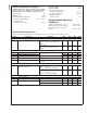

Absolute Maximum Ratings (Note 1)
If Military/Aerospace specified devices are required,
please contact the National Semiconductor Sales
Office/Distributors for availability and specifications.
Supply Voltage 4V
Output Current 27 mA
Maximum Junction Temperature +125˚C
Storage Temperature Range −65˚C to +150˚C
Lead Temperature
(Soldering 10 seconds) +300˚C
ESD Rating (HBM) ≥ 7kV
ESD Rating (MM) ≥ 500V
Package Thermal Resistance
θ
JA
Surface Mount AJE 125˚C/W
θ
JC
Surface Mount AJE 105˚C/W
Reliability Information
Transistor count 291
Recommended Operating
Conditions
Supply Voltage Range (V
DD
-V
SS
) +3.0V to +3.6V
Operating Free Air Temperature (T
A
) -40˚C to +85˚C
R
BB
Range (applied to V
BB
input)
(Note 6) 1.3kΩ to 11.5kΩ
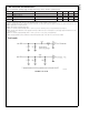
Electrical Characteristics
Over recommended operating supply and temperature ranges unless otherwise specified (Notes 2 and 3)
Symbol Parameter Conditions Min Typ Max Units
OUTPUT DC SPECIFICATIONS
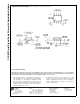
V
SDO
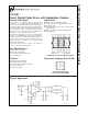
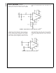
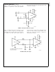
Serial Driver Output Voltage R
L
=75Ω1%,
R
REF
= 1.91 kΩ 1% (for 800 mV
p-p
),
Figure 1
720 800 880 mV
R
L
=75Ω1%,
R
REF
= 1.5 kΩ 1% (for 1.0 V
p-p
),
Figure 1
900 1000 1100 mV
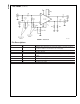
INPUT DC SPECIFICATIONS
V
TH
Differential Input High Threshold V
CM
= +0.05V or +1.2V or +3.25V, 0 +100 mV
V
TL
Differential Input Low Threshold V
DD
= 3.3V −100 0 mV
V
CMR
Common Mode Voltage Range V
ID
= 100mV, V
DD
= 3.3V 0.05 3.25 V
I
IN
Input Current V
IN
= 0V or +3.0V, V
DD
= 3.6V or 0V
±
1
±
10 µA
I
INB
Input Current Balance V
IN
= 0V or +3.0V, V
DD
= 3.6V or 0V,
(Note 8)
0.23 µA
SUPPLY CURRENT
I
DD
Total Dynamic Power Supply Current
(includes load current)
R
L
=75Ω,
R
REF
= 1.91 kΩ 1%
(V
SDO
= 800 mV
p-p
@
270 Mbps)
70 115 mA
R
L
=75Ω,
R
REF
= 1.5 kΩ 1%
(V
SDO
= 1.0 V
p-p
@
622 Mbps)
85 130 mA
MISCELLANEOUS PARAMETERS
L
GEN
Output Inductance 6nH
R
GEN
Output Resistance 25 kΩ
I
BB
V
BB
Current R
REF
= 1.91 kΩ 1%, (Note 6) 250 µA
R
REF
= 1.5 kΩ 1%, (Note 6) 315 µA
CLC001
www.national.com 2