
Owner manual
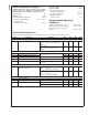

AC Electrical Characteristics
Over recommended operating supply and temperature ranges unless otherwise specified (Note 3)
Symbol Parameter Conditions Min Typ Max Units
t
r
,t
f
Rise time, Fall time 20%–80%, (Notes 4, 5) 400 800 ps
t
os
Output overshoot 5%
t
jit
Output jitter (Note 7) 25 ps
t
pd
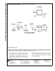
Propagation delay (Note 5) 1.9 ns
Note 1: “Absolute Maximum Ratings” are those values beyond which the safety of the device cannot be guaranteed. They are not meant to imply that the devices
should be operated at these limits. The table of “Electrical Characteristics” specifies conditions of device operation.
Note 2: Current flow into device pins is defined as positive. Current flow out of device pins is defined as negative. All voltages are stated referenced to V
SS
=0V.
Note 3: Typical values are at 25˚C and 3.3V.
Note 4: This parameter is Guaranteed by Design.
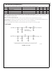
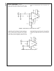
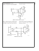
Note 5: R
L
=75Ω, AC-coupled at 270 Mbps, R
REF
= 1.91 kΩ 1% (for V
SDO
= 800 mV
p-p
±
10%), C
L
not greater than 5pF (See
Figure 1
)
Note 6: The V
BB
output is intended as a bias supply pin for the inputs of this device only. It is not designed as a power supply output and should not be used to
power other devices.
Note 7: R
L
=75Ω, AC-coupled at 622 Mbps, R
REF
= 1.5 kΩ 1% (for V
SDO
= 1.0 V
p-p
±
10%), clock pattern input.
Note 8: Input Current Balance (I
INB
) is the difference between the Input Current (I
IN
)onV
IN+
and V
IN−
for the same bias condition.
Test Loads
DS101329-4
FIGURE 1. Test Loads
CLC001
www.national.com3