
Owner manual

Device Operation
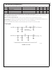
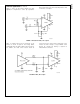
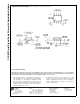
INPUT INTERFACING
Numerous input configurations exist for applying PECL,
LVPECL, and LVDS signals to the input of the CLC001.
Inputs may be single-ended or differential, AC or DC
coupled.
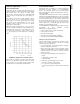
The V
BB
pin may be used to provide a DC bias voltage to
the inputs. Leave this pin as a no connect when no bias is
needed. Note that DC-coupled inputs such as direct
LVDS and LVPECL connections are self-biasing and do
not require use of the V
BB
pin. I
BB
, the current produced
by the V
BB
pin, depends on R
REF
. For a given R
REF
, the
I
BB
current will remain constant, and the bias voltage is
determined by the value of resistance, R
BB
, between the
V
BB
pin and ground.
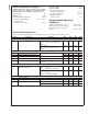
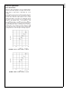
Figure 3
and
Figure 4
show how R
BB
corresponds to some common V
BB
values with R
REF
held
at 1.91 kΩ and 1.5 kΩ, respectively. Some common input
configurations are shown in
Figure 5
through
Figure 9
.
DS101329-11
FIGURE 3. R
BB
vs. V
BB
for R
REF
= 1.91 kΩ
DS101329-12
FIGURE 4. R
BB
vs. V
BB
for R
REF
= 1.5 kΩ
CLC001
www.national.com5