
Owner manual

Device Operation (Continued)
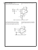
OUTPUT INTERFACING
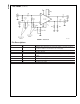
The CLC001 has two complementary, ground referenced
outputs designed to drive AC-coupled and terminated
75Ω coaxial cables. The outputs are single ended;
however, they could be treated as a single differential
output as long as current paths from each output go to
ground.
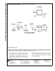
The output of the CLC001 is a high impedance current
source. It expects to see a 75Ω shunt resistor before
driving cable to convert the current output to a voltage
and provide proper back-matching. No series back-
matching resistors should be used. Refer to
Typical
Application
for an illustration.
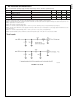
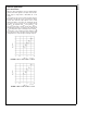
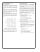
Output levels range from 800 mV
p-p
to 1.0 V
p-p
±
10% into
75Ω AC-coupled, back-matched loads. Output level is
controlled by the value of R
REF
connected to pin 4. R
REF
is 1.91 kΩ
±
1% for 800 mV
p-p
, and 1.5 kΩ
±
1% for 1.0
V
p-p
. Refer to
Figure 10
for the output level’s sensitivity to
R
REF
.
The CLC001 is designed as an AC-coupled 75Ω cable
driver. It is not intended to drive 50Ω loads. The current
source output does not provide enough current to allow
for 800mV across a 50Ω doubly terminated load.
Evaluation Board
Evaluation boards are available for a nominal charge that
demonstrate the basic operation of the SDI/SDV/SDH
devices. The evaluation boards can be ordered through
National’s Distributors. Supplies are limited, please check for
current availability.
The SD001EVK evaluation kit for the CLC001, Serial Digital
Cable Driver with Adjustable Outputs, provides an operating
environment in which the cable driver can be evaluated by
system / hardware designers. The evaluation board has all
the needed circuitry and connectors for easy connection and
checkout of the device circuit options as discussed in the
CLC001 datasheet. A schematic, parts list and pictorial
drawing are provided with the board.
From the WWW, the following information may be viewed /
downloaded for most evaluation boards:
www.national.com/appinfo/interface
•
Device Datasheet and / or EVK User Manual
•
View a picture of the EVK
•
View the EVK Schematic
•
View the top assembly drawing and BOM
•
View the bottom assembly drawing and BOM
PCB Layout Recommendations
Printed circuit board layout affects the performance of the
CLC001. The following guidelines will aid in achieving
satisfactory device performance.
•
Use a ground plane or power/ground plane sandwich
design for optimum performance.
•
Bypass device power with a 0.01 µF monolithic ceramic
capacitor in parallel with a 6.8 µF tantalum electrolytic
capacitor located no more than 0.1″ (2.5 mm) from the
device power pins.
•
Provide short, symmetrical ground return paths for:
— inputs,
— supply bypass capacitors and
— the output load.
•
Provide short, grounded guard traces located
— under the centerline of the package,
— 0.1″ (2.5 mm) from the package pins
— on both top and bottom of the board with connecting
vias.
DS101329-13
FIGURE 10. Output level’s sensitivity to R
REF
CLC001
www.national.com9