
User Manual


DS2401
10 of 10
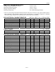
NOTES:
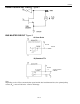
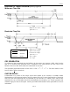
1) All voltages are referenced to ground.
2) V
PUP
= external pullup voltage.
3) Input load is to ground.
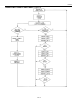
4) An additional reset or communication sequence cannot begin until the reset high time has expired.
5) Read data setup time refers to the time the host must pull the 1-Wire bus low to read a bit. Data is
guaranteed to be valid within 1ms of this falling edge and will remain valid for 14ms minimum (15ms
total from falling edge on 1-Wire bus).
6) V
IH
is a function of the external pullup resistor and the V
CC
supply.
7) 30 nanocoulombs per 72 time slots @ 5.0V.
8) At V
CC
= 5.0V with a 5kW pullup to V
CC
and a maximum time slot of 120ms.
9) Capacitance on the I/O pin could be 800pF when power is first applied. If a 5kW resistor is used to
pullup the I/O line to V
CC
, 5ms after power has been applied the parasite capacitance will not affect
normal communications.
10) The reset low time (t
RSTL
) should be restricted to a maximum of 960ms, to allow interrupt signaling,
otherwise it could mask or conceal interrupt pulses if this device is used in parallel with a DS2404 or
DS1994.
11) Under certain low voltage conditions, V
ILMAX
may have to be reduced to as much as 0.5V to always
guarantee a Presence Pulse.
12) The optimal sampling point for the master is as close as possible to the end time of the t
RDV
period
without exceeding t
RDV
. For the case of a Read-One Time slot, this maximizes the amount of time for
the pullup resistor to recover to a high level. For a Read-Zero Time slot, it ensures that a read will
occur before the fastest 1-Wire device(s) releases the line.
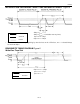
13) The duration of the low pulse sent by the master should be a minimum of 1µs with a maximum value
as short as possible to allow time for the pullup resistor to recover the line to a high level before the 1-
Wire device samples in the case of a Write-One Time or before the master samples in the case of a
Read-One Time.