
Manual


DS2740
3 of 15
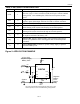
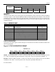
Table 2. DETAILED PIN DESCRIPTION
PIN SYMBOL DESCRIPTION
OVD 1
1-Wire Bus Speed Control. Input logic level selects the speed of the 1-
Wire bus. Logic 1 selects overdrive (OVD) and Logic 0 selects standard
timing (STD). On a multidrop bus, all devices must operate at same
speed.
PIO 2
Programmable I/O Pin. Programmed as input or output through internal
registers. Open-drain output sufficient for LED or vibrator activation.
SNS 3
Current-Sense Resistor Input
IS2
4
Current-Sense Input. Connected to SNS through a 10kΩ resistor to
allow filtering of the current waveform by an external capacitor.
IS1 5
Current-Sense Input. Connected to V
SS
through a 10kΩ resistor to allow
filtering of the current waveform through an external capacitor.
V
SS
6
Device Ground, Current-Sense Resistor Return. Connect directly to
the negative terminal of the battery cell.
DQ 7
Data I/O Pin. Operates bidirectionally with open-drain output driver.
Internal 1µA pulldown aids in sensing pack removal and sleep-mode
activation.
V
DD
8
Power-Supply Input. Connects to system voltage supply or positive
terminal of battery cell.
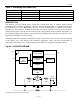
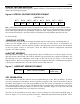
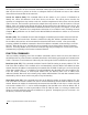
Figure 2. APPLICATION EXAMPLE
DS2740
VDD
VSS
DQ
PIO
DATA
2.7V to 5.5V
System Supply
Battery Pack
Ne
g
ative
Battery
Pack
Return
SNS
PIO
IS1IS2
104
150
150
R
SNS
104
System
GND
OVD
* *
* 5.6V zener recommended for ESD protection when DATA or PIO
contacts exposed, such as a removable battery pack application
150