
Manual


DS2740
6 of 15
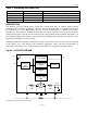
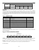
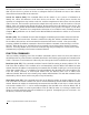
ACR RANGE
R
SNS
PART
V
IS1
- V
IS2
20mW 15mW 10mW 5mW
DS2740
DS2740B
±204.8mVh ±10.24Ah ±13.65Ah ±20.48Ah ±40.96Ah
MEMORY
The DS2740 has memory space with registers for instrumentation, status, and control. When the MSB of
a two-byte register is read, both the MSB and LSB are latched and held for the duration of the read data
command to prevent updates during the read and ensure synchronization between the two register bytes.
For consistent results, always read the MSB and the LSB of a two-byte register during the same read data
command sequence.
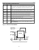
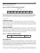
Table 3. MEMORY MAP
ADDRESS (HEX) DESCRIPTION READ/WRITE
00 Reserved —
01 Status Register R
02 to 07 Reserved —
08 Special Feature Register R/W
09 to 0D Reserved —
0E Current Register MSB R
0F Current Register LSB R
10 Accumulated Current Register MSB R/W
11 Accumulated Current Register LSB R/W
12 to FF Reserved —
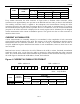
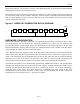
STATUS REGISTER
The format of the status register is shown in Figure 5. The function of each bit is described in detail in the
following paragraphs.
Figure 5. STATUS REGISTER FORMAT
ADDRESS 01
BIT 7 BIT 6 BIT 5 BIT 4 BIT 3 BIT 2 BIT 1 BIT 0
X SMOD X RNAOP X X X X
SMOD—SLEEP Mode Enable. A value of 1 allows the DS2740 to enter sleep mode when DQ is low for
2s. A value of 0 disables DQ related transitions to sleep mode. The power-up default of SMOD = 0.
RNAOP—Read Net Address Opcode. A value of 0 in this bit sets the opcode for the read net address
command to 33h, while a 1 sets the opcode to 39h. The power-up default of RNAOP = 0.
X—Reserved bits.