
Owner's manual


__________Applications Information
Rail-to-Rail Inputs and Outputs
The MAX4162/MAX4163/MAX4164 input common-mode
range extends 250mV beyond each of the supply rails,
providing a substantial increase in dynamic range over
other op amps (even many of those referred to as rail-to-
rail). Although the minimum operating voltage is speci-
fied at 2.7V, the devices typically provide full rail-to-rail
operation below 2.0V (Figure 1). These amplifiers do not
suffer from midswing common-mode-rejection degrada-
tion or crossover nonlinearity often encountered in other
rail-to-rail op amps. Extremely low, 1.0pA input bias cur-
rent makes these devices ideal for applications such as
pH probes, electrometers, and ionization detectors.
They are also protected against phase reversal (inferred
from CMRR test) and latchup for input signals extending
beyond the supply rails. The output stage achieves a
lower output impedance than traditional rail-to-rail out-
put stages, providing an output voltage range that typi-
cally swings within 150mV of the supply rails for 1mA
loads. This architecture also maintains high open-loop
gain and output swing while driving substantial loads.
Output Loading and Stability
These devices drive 1mA loads to within 150mV of the
supply rails while consuming only 25µA of quiescent
current. Internal compensation allows these amplifiers to
remain unity-gain stable while driving any capacitive
load (Figure 2).
Internal Charge Pump
An internal charge pump provides two internal supplies
typically 2V beyond each rail. These internal rails allow
the MAX4162/MAX4163/MAX4164 to achieve true rail-
to-rail inputs and outputs, while providing excellent
common-mode rejection, power-supply rejection ratios,
and gain linearity.
These charge pumps require no external components,
and in most applications are entirely transparent to the
user. Two characteristics may be visible to the user,
depending on the application:
MAX4162/MAX4163/MAX4164
UCSP, Micropower, Single-Supply, 10V,
Rail-to-Rail I/O Op Amps
10 ______________________________________________________________________________________
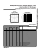
IN
200mV/div
500mV
0
500mV
0
OUT
200mV/div
LARGE CAPACITIVE-LOAD DRIVE
MAX4162-36
5µs/div
A
V
= 1, C
L
= 1µF, R
L
= 100kΩ
Figure 2. Large Capacitive-Load Drive
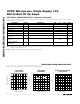
IN
0.667V/div
2V
0
2V
0
OUT
0.667V/div
RAIL-TO-RAIL
INPUT/OUTPUT VOLTAGE RANGE
(V
DD
= 2V)
MAX4162-34
200µs/div
V
DD
= 2V, V
P-P
= 2V, f = 1kHz, R
L
= 10kΩ
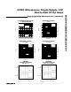
Figure 1. Rail-to-Rail I/O: a) V
DD
= 3V; b) V
DD
= 2V
IN
1V/div
3V
0
3V
0
OUT
1V/div
RAIL-TO-RAIL
INPUT/OUTPUT VOLTAGE RANGE
(V
DD
= 3V)
MAX4162-35
200µs/div
V
DD
= 3V, V
P-P
= 3V, f = 1kHz, R
L
= 10kΩ
a)
b)