
Owner's manual


MAX4162/MAX4163/MAX4164
UCSP, Micropower, Single-Supply, 10V,
Rail-to-Rail I/O Op Amps
2 _______________________________________________________________________________________
ABSOLUTE MAXIMUM RATINGS
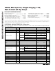
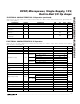
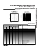
ELECTRICAL CHARACTERISTICS: 3V Operation
(V
DD
= 3V, V
SS
= 0, V
CM
= V
DD
/2, V
OUT
= V
DD
/2, R
L
tied to V
DD
/2, T
A
= -40°C to +85°C, unless otherwise noted. Typical values are
at T
A
= +25°C.) (Note 1)
Stresses beyond those listed under “Absolute Maximum Ratings” may cause permanent damage to the device. These are stress ratings only, and functional
operation of the device at these or any other conditions beyond those indicated in the operational sections of the specifications is not implied. Exposure to
absolute maximum rating conditions for extended periods may affect device reliability.
Supply Voltage (V
DD
to V
SS
)..................................................11V
IN+, IN-, OUT Voltage ......................(V
DD
+ 0.3V) to (V
SS
- 0.3V)
Short-Circuit Duration (to either rail)...........................Continuous
Continuous Power Dissipation (T
A
= +70°C)
5-Pin SOT23 (derate 7.1mW/°C above +70°C)..............571mW
8-Pin SO (derate 5.88mW/°C above +70°C)..................471mW
8-Pin UCSP (derate 4.7mW/°C above +70°C) ...............379mW
8-Pin µMAX (derate 4.1mW/°C above +70°C) ...............330mW
14-Pin SO (derate 8.00mW/°C above +70°C)................640mW
Operating Temperature Range ...........................-40°C to +85°C
Storage Temperature Range .............................-65°C to +150°C
Junction Temperature......................................................+150°C
Lead Temperature (soldering, 10s) .................................+300°C
To either supply rail
V
OL
- V
SS
V
DD
- V
OH
V
OL
- V
SS
V
DD
- V
OH
Inferred from PSRR test
R
L
= 10kΩ
Inferred from CMRR test
T
A
= +25°C
T
A
= -40°C to +85°C
T
A
= +25°C
T
A
= -40°C to +85°C
CONDITIONS
15I
SC
mV
325
R
L
= 100kΩ
V
OUT
325
30 180
R
L
= 10kΩ
30 180
dBA
V
85 120
dBCMRR 70 100
pA1.0 100
V2.7 10.0V
DD
I
B
TΩ
V
SS
- V
DD
+
0.25 0.25
V
CM
>10R
IN
±6
±0.5 ±5
MAX4164
±0.5 ±3
V
OS
±4
MAX4162
±0.5 ±4
mV
±5
MAX4163
UNITSMIN TYP MAXSYMBOL
A
V
= 1V/V
kHz200GBWP
V
DD
= 2.7V to 10VPSRR dB80 110
mA
0.1R
OUT
V
V
CM
= (V
SS
- 0.25V) to (V
DD
+ 0.25V)
Ω
µV/°CTCV
OS
2
T
A
= +25°C
T
A
= -40°C to +85°C
µA25 40I
DD
degrees60
φM
dB12GM
V
OUT
= 1V to 2V step µs50
V
DD
= 0 to 3V step, V
IN
= V
DD
/2, A
V
= 1V/V µs20t
ON
V/ms115SR
f = 1kHz, V
OUT
= 2V
P-P
, R
L
= 100kΩ, A
V
= 1V/VTHD %0.02
Phase Margin
Gain Margin
Output Short-Circuit Current
Output Voltage Swing
Input Offset Voltage Tempco
Settling Time to 0.1%
Large-Signal Voltage Gain
Supply Current (Per Amplifier)
Turn-On Time
Slew Rate
Total Harmonic Distortion
Common-Mode Rejection Ratio
Operating Voltage Range
Input Bias Current (Note 2)
Input Common-Mode Voltage
Range
Differential Input Resistance
Input Offset Voltage
PARAMETER
Gain-Bandwidth Product
Power-Supply Rejection Ratio
Closed-Loop Output Resistance