
Owner's manual


MAX4162/MAX4163/MAX4164
UCSP, Micropower, Single-Supply, 10V,
Rail-to-Rail I/O Op Amps
4 _______________________________________________________________________________________
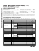
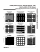
0
5
10
15
20
25
30
1234567
8
9
10
SUPPLY CURRENT
vs. SUPPLY VOLTAGE
MAX4162-01
SUPPLY VOLTAGE (V)
SUPPLY CURRENT (µA)
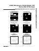
10
12
14
16
18
20
22
24
26
28
-40 -20 0 20
40
60 80 100
SUPPLY CURRENT
vs. TEMPERATURE
MAX4162-02
TEMPERATURE (°C)
SUPPLY CURRENT (µA)
V
CC
= 5V
V
CC
= 3V
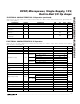
-150
-130
-110
-90
-70
-50
-30
-10
10
30
50
12345678910
INPUT OFFSET VOLTAGE VARIATION
vs. SUPPLY VOLTAGE
MAX4162-03
SUPPLY VOLTAGE (V)
V
OS
(µV)
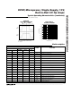
ELECTRICAL CHARACTERISTICS: 5V Operation (continued)
(V
DD
= 5V, V
SS
= 0, V
CM
= V
DD
/2, V
OUT
= V
DD
/2, R
L
tied to V
DD
/2, T
A
= -40°C to +85°C, unless otherwise noted. Typical
values are at T
A
= +25°C.) (Note 1)
__________________________________________Typical Operating Characteristics
(V
DD
= 5V, V
SS
= 0, V
CM
= V
DD
/2, T
A
= +25°C, unless otherwise noted.)
Note 1: All device specifications are 100% tested at T
A
= +25°C. Limits over the extended temperature range are guaranteed by
design, not production tested.
Note 2: Input bias current guaranteed by design, not production tested.
pF
CONDITIONS
%THD 0.02f = 1kHz, V
OUT
= 2V
P-P
, R
L
= 100kΩ, A
V
= 1V/VTotal Harmonic Distortion
Input Common-Mode
Capacitance
V/ms
1.5
Slew Rate 115
PARAMETER
SR
kHz
Internal Charge-Pump
Frequency
700
µV
P-P
Charge-Pump Output
Feedthrough
100
UNITSMIN TYP MAXSYMBOL
V
OUT
= 1V to 2V step µsSettling Time to 0.1% 70
V
DD
= 0 to 3V step, V
IN
= V
DD
/2, A
V
= 1V/V µsTurn-On Time 40t
ON
f = 1kHz
nV/
√
Hz
Input Voltage-Noise Density 80e
n
pFDifferential Input Capacitance 0.7