
User Manual
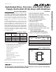

MAX4165–MAX4169
High-Output-Drive, Precision, Low-Power, Single-
Supply, Rail-to-Rail I/O Op Amps with Shutdown
10 ______________________________________________________________________________________
Single-Supply Speaker Driver
The MAX4165/MAX4166 can be used as a single-sup-
ply speaker driver, as shown in the
Typical Operating
Circuit
. Capacitor C1 is used for blocking DC (a 0.1µF
ceramic capacitor can be used). When choosing resis-
tors R3 and R4, take into consideration the input bias
current as well as how much supply current can be tol-
erated. Choose resistors R1 and R2 according to the
amount of gain and current desired. Capacitor C3
ensures unity gain for DC. A 10µF electrolytic capacitor
is suitable for most applications. The coupling capaci-
tor C2 sets a low-frequency pole and is fairly large in
value. For a 32Ω load, a 100µF coupling capacitor
gives a low-frequency pole at 50Hz. The low-frequency
pole can be set according to the following equation:
ƒ = 1 / 2π (R
L
C2)
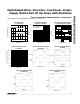
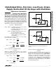
Bridge Amplifier
The circuit shown in Figure 3 uses a dual MAX4167/
MAX4168 to implement a 3V, 200mW amplifier suitable
for use in size-constrained applications. This configura-
tion eliminates the need for the large coupling capaci-
tor required by the single op-amp speaker driver when
single-supply operation is a must. Voltage gain is set to
+10V/V; however, it can be changed by adjusting the
900kΩ resistor value. DC voltage at the speaker is limit-
ed to 10mV. The 47Ω and 0.1µF capacitors across the
speaker maintain a low impedance at the load as fre-
quency increases.
Rail-to-Rail Input Stage
Devices in the MAX4165–MAX4169 family of high-out-
put-current amplifiers have rail-to-rail input and output
stages designed for low-voltage, single-supply opera-
tion. The input stage consists of separate NPN and
PNP differential stages that combine to provide an
input common-mode range that extends 0.25V beyond
the supply rails. The PNP stage is active for input volt-
ages close to the negative rail, and the NPN stage is
active for input voltages near the positive rail. The
switchover transition region, which occurs near V
CC
/ 2,
has been extended to minimize the slight degradation
in common-mode rejection ratio caused by mismatch of
the input pairs.
V
CC
= +3V
900k
V
CC
= +3V
V
CC
= +3V
47Ω
4.7k
4.7k
0.1µF
1µF
0.1µF
INPUT
0.25Vp-p
32Ω
100k
100k
100k
100k
100k
100k
1/2 MAX4167
1/2 MAX4168
1/2 MAX4167
1/2 MAX4168
Figure 3. Dual MAX4167/MAX4168 Bridge Amplifier for
200mW at 3V
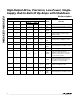
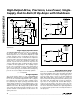
R3
R3 = R1 R2
R1 R2
MAX4165
MAX4166
MAX4167
MAX4168
MAX4169
Figure 4. Reducing Offset Error Due to Bias Current
(Noninverting)
R3
R3 = R1 R2
R1 R2
MAX4165
MAX4166
MAX4167
MAX4168
MAX4169
Figure 5. Reducing Offset Error Due to Bias Current (Inverting)