
User Manual


MAX4165–MAX4169
High-Output-Drive, Precision, Low-Power, Single-
Supply, Rail-to-Rail I/O Op Amps with Shutdown
______________________________________________________________________________________ 11
Since the input stage switches between the NPN and
PNP pairs, the input bias current changes polarity as the
input voltage passes through the transition region. Match
the effective impedance seen by each input to reduce the
offset error caused by input bias currents flowing through
external source impedances (Figures 4 and 5).
High source impedances, together with input capaci-
tance, can create a parasitic pole that produces an
underdamped signal response. Reducing the input
impedance or placing a small (2pF to 10pF) capacitor
across the feedback resistor improves response.
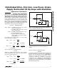
The MAX4165–MAX4169’s inputs are protected from large
differential input voltages by 1kΩ series resistors and
back-to-back triple diodes across the inputs (Figure 6).
For differential voltages less than 1.8V, input resistance is
typically 500kΩ. For differential input voltages greater
than 1.8V, input resistance is approximately 2kΩ. The
input bias current is given by the following equation:
I
BIAS
= (V
DIFF
- 1.8V) / 2kΩ
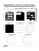
Rail-to-Rail Output Stage
The minimum output is within millivolts of ground for
single-supply operation, where the load is referenced
to ground (V
EE
). Figure 7 shows the input voltage range
and the output voltage swing of a MAX4165 connected
as a voltage follower. The maximum output voltage
swing is load dependent; however, it is guaranteed to
be within 430mV of the positive rail (V
CC
= 5V) even
with maximum load (25Ω to ground).
Driving Capacitive Loads
The MAX4165–MAX4169 have a high tolerance for
capacitive loads. They are stable with capacitive loads
up to 250pF. Figure 8 is a graph of the stable operating
region for various capacitive loads vs. resistive loads.
Figures 9 and 10 show the transient response with
excessive capacitive loads (1500pF), with and without
the addition of an isolation resistor in series with the
output. Figure 11 shows a typical noninverting capaci-
tive-load-driving circuit in the unity-gain configuration.
The resistor improves the circuit’s phase margin by iso-
lating the load capacitor from the op amp’s output.
1k
1k
Figure 6. Input Protection Circuit
IN
(1V/div)
OUT
(1V/div)
MAX4165-fig07
TIME (5µs/div)
V
CC
= +3.0V
R
L
= 100kΩ
Figure 7. Rail-to-Rail Input/Output Range