
User Manual

MAX4165–MAX4169
High-Output-Drive, Precision, Low-Power, Single-
Supply, Rail-to-Rail I/O Op Amps with Shutdown
2 _______________________________________________________________________________________
ABSOLUTE MAXIMUM RATINGS
Stresses beyond those listed under “Absolute Maximum Ratings” may cause permanent damage to the device. These are stress ratings only, and functional
operation of the device at these or any other conditions beyond those indicated in the operational sections of the specifications is not implied. Exposure to
absolute maximum rating conditions for extended periods may affect device reliability.
Supply Voltage (V
CC
to V
EE
)....................................................7V
IN_+, IN_-,
SHDN_............................(V
EE
- 0.3V) + (V
CC
+ 0.3V)
OUT_ (shutdown mode) ...................(V
EE
- 0.3V) + (V
CC
+ 0.3V)
Output Short-Circuit Duration to V
CC
or V
EE
(Note 1)....Continuous
Continuous Power Dissipation (T
A
= +70°C)
5-Pin SOT23 (derate 7.10mW/°C above +70°C)...........571mW
8-Pin Plastic DIP (derate 9.09mW/°C above +70°C) ....727mW
8-Pin SO (derate 5.88mW/°C above +70°C).................471mW
8-Pin µMAX (derate 4.10mW/°C above +70°C)............330mW
10-Pin µMAX (derate 5.60mW/°C above +70°C)..........444mW
14-Pin Plastic DIP (derate 10.00mW/°C above +70°C)...800mW
14-Pin SO (derate 8.33mW/°C above +70°C)...............667mW
Operating Temperature Range ...........................-40°C to +85°C
Junction Temperature......................................................+150°C
Storage Temperature Range.............................-65°C to +150°C
Lead Temperature (soldering, 10sec).............................+300°C
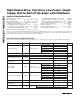
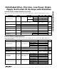
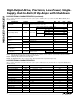
DC ELECTRICAL CHARACTERISTICS
(V
CC
= +2.7V to +6.5V, V
EE
= 0V, V
CM
= 0V, V
OUT
= (V
CC
/ 2), R
L
= 100kΩ to (V
CC
/ 2), V
SHDN
≥ 2V, T
A
= +25°C, unless otherwise
noted.)
| V
IN
+ - V
IN
- | > 1.8V
| V
IN
+ - V
IN
- | ≤ 1.8V
V
CM
= V
EE
to V
CC
Inferred from CMRR test
CONDITIONS
2
R
IN(DIFF)
Differential Input Resistance kΩ
500
nA±1 ±15I
OS
Input Offset Current
VV
EE
- 0.25 V
CC
+ 0.25V
CM
Common-Mode Input
Voltage Range
V
SHDN
< 0.8V, V
OUT
= 0V to V
CC
A
VCL
= +1V/V
V
OUT
= 0.2V to 4.8V, R
L
= 100kΩ
µA±0.001 ±2I
OUT(SHDN)
Off-Leakage Current
in Shutdown
Ω0.1R
OUT
Output Resistance
72 93
72 93
MAX416_EPA/EPD
MAX416_ESA/ESD
0.35 1.5
0.25 0.85
V
CC
= 5VA
VOL
Large-Signal Voltage Gain
95 120
UNITSMIN TYP MAXSYMBOLPARAMETER
MAX416_EPA/EPD
0.25 0.85MAX416_ESA/ESD
V
CM
= V
EE
to V
CC
mV0.35 1.7V
OS
Input Offset Voltage MAX416_EUA/EUB
0.25 1.0
MAX416_EUK
MAX416_EUA/EUB
72 86
72 88
63 90
62 89
MAX416_EUK
MAX416_ESA/ESD
72 86
MAX416_EUA/EUB
70 88
MAX416_EUK
MAX4169E_D
V
CC
= 2.7V to 6.5VPSRRPower-Supply Rejection Ratio dB
V
OUT
= 0.6V to 4.4V, R
L
= 25Ω 71 83
dB
Note 1: Continuous power dissipation should also be observed.
71 93
dB
V
EE
- 0.25V <
V
CM
< (V
CC
+ 0.25V)
CMRR
Common-Mode
Rejection Ratio
72 88MAX416_EPA/EPD
V
CM
= V
EE
to V
CC
nA±50 ±150I
B
Input Bias Current
MAX4169E_D
MAX4169E_D