
User Manual

MAX4165–MAX4169
High-Output-Drive, Precision, Low-Power, Single-
Supply, Rail-to-Rail I/O Op Amps with Shutdown
_______________________________________________________________________________________ 9
Applications Information
Package Power Dissipation
Warning: Due to the high output current drive, this op
amp can exceed the absolute maximum power-dissi-
pation rating. As a general rule, as long as the peak cur-
rent is less than or equal to 80mA, the maximum package
power dissipation will not be exceeded for any of the
package types offered. There are some exceptions to this
rule, however. The absolute maximum power-dissipation
rating of each package should always be verified using
the following equations. The following equation gives an
approximation of the package power dissipation:
where: V
RMS
= the RMS voltage from V
CC
to V
OUT
when sourcing current
= the RMS voltage from V
OUT
to V
EE
when sinking current
I
RMS
= the RMS current flowing out of or into
the op amp and the load
θ = the phase difference between the
voltage and the current. For resistive
loads, COS θ = 1.
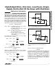
For example, the circuit in Figure 1 has a package
power dissipation of 157mW.
Therefore, P
IC(DISS)
= V
RMS
I
RMS
COS θ
= 157mW
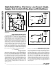
Adding a coupling capacitor improves the package
power dissipation because there is no DC current to
the load, as shown in Figure 2.
Therefore, P
IC(DISS)
= V
RMS
I
RMS
COS θ
= 38.6mW
The absolute maximum power-dissipation rating of this
package would be exceeded if the configuration in
Figure 1 were used with all four of the MAX4169ESD’s
amplifiers at a high ambient temperature of +75°C
(157mW x 4 amplifiers = 628mW + a derating of
8.33mW/°C x 5°C = 669mW). Note that 669mW just
exceeds the absolute maximum power dissipation of
667mW for the 14-pin SO package (see the
Absolute
Maximum Ratings
section).
V V V
I +
I
2
RMS CC DC
RMS
PEAK
≅ −
( )
−
= − − =
≅ = +
=
. .
.
.
. /
.
V
V V
V
V
I A
V
mA
PEAK
RMS
DC
RMS
2
6 5 3 25
1 5
2
2 189
0
1 5 60
2
17 67
Ω
V V V
I +
I
2
RMS CC DC
RMS
PEAK
≅ −
( )
−
= − − =
≅ = +
=
. .
.
.
.
. /
.
V
V V
V
V
I
V V
mA
PEAK
RMS
DC
RMS
2
6 5 3 25
1 5
2
2 189
3 25
60
1 5 60
2
71 84
Ω
Ω
P V I COS
IC DISS RMS RMS
( )
≅ θ
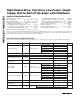
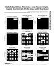
6.5V
V
IN
= 3Vp-p
R
C
60Ω
R
MAX4165
MAX4166
Figure 1. A Circuit Example where the MAX4165/MAX4166 is
Being Used in Single-Supply Operation
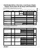
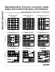
6.5V
V
IN
= 3Vp-p
R
60Ω
R
C
C
C
C
C
= 1
2π R
L
f
L
MAX4165
MAX4166
Figure 2. A Circuit Example where Adding a Coupling
Capacitor Greatly Reduces the Power Dissipation of Its
Package