EDK3687 USER MANUAL FOR H8/3687 ON-CHIP FLASH MICROCONTROLLER
Preface Cautions 1. This document may be, wholly or partially, subject to change without notice. 2. All rights reserved. No one is permitted to reproduce or duplicate, in any form, a part or this entire document without Renesas Technology Europe Limited's written permission. Trademarks General All brand or product names used in this manual are trademarks or registered trademarks of their respective companies or organisations.
1. TABLE OF CONTENTS 1. TABLE OF CONTENTS ............................................................................................................................................. 3 2. START-UP INSTRUCTIONS ....................................................................................................................................... 4 2.1. INSTALLING THE EVALUATION DEVELOPMENT KIT (EDK)........................................................................... 4 2.2. SERIAL CONNECTION ....
2. START-UP INSTRUCTIONS 2.1. INSTALLING THE EVALUATION DEVELOPMENT KIT (EDK) Please refer to the quick start guide provided for initial installation of the EDK. A copy of the quick start guide and other information relating to this EDK at: http://www.eu.renesas.com/tools Installing the EDK requires power and serial connection to a host computer. 2.2. SERIAL CONNECTION The serial communications cable for connecting the EDK to a host computer requires 1:1 connectivity.
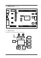
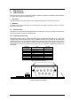
3. EDK BOARD LAYOUT The diagram shows a general layout of the EDK board. J1 UVcc GND Testpoints RESn FW NMIn ULED1 ULED2 PSCK PTXD PRXD RX232 TX232 NMI Switch Power LED User1 LED User2 LED LIN LIN 5V OSC Microprocessor XTAL RESET Switch SPI DEBUG Power CTS RTS 9-Way D-Type I2C I2C FLASH Programming J2 CJ4 FIGURE 3-1: EDK BOARD LAYOUT 3.1. EDK BLOCK DIAGRAM The diagram shows the connectivity of the components on the EDK board.
4. EDK OPERATION 4.1. USER INTERFACE The EDK provides two buttons for influencing the operation of the board. The purpose of each button is clearly marked next to it. Refer to the board layout for positions (Section 3) 1. Reset Switch This button provides the microcontroller with a reset pulse utilizing the built in power on reset control of the device. 2. NMI Switch This button provides a de-bounced signal to the microcontroller for each operation of the button.
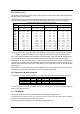
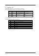
4.2.2. CRYSTAL CHOICE The operating crystal frequency has been chosen to support the fastest operation with the fastest serial operating speeds. The value of the crystal is 18.432MHz. The following table shows the baud rates and Baud Rate Register (BRR) setting required for each communication rate using the above default operating speed. It also confirms the resultant baud rate and the bit error rate that can be expected. Baud Rate Register Settings for Serial Communication Rates SMR 0 Setting: Comm.
4.4. I2C EEPROM The board has been tested with an Atmel AT24C04AN-10SI-2.7 I2C EEPROM device (Not supplied). The device is configured to connect to dedicated I2C pins on Ports P56 and P57. 4.5. LIN INTERFACE The board has been tested with an Philips TJA1020TD device (Not supplied). The device should be connected to P71 and P72 using 0R links on R29 and R31. Alternative connections are available; refer to section 5.3 for more information.
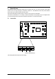
5. BOARD OPTIONS The EDK has a number of configuration settings set by four jumpers CJ4 (A, B, C, D) and zero-ohm links. Common EDK functions can be set using the jumpers as described in sections 5.2. The additional zero-ohm links provide additional features that may be required to interface with other systems. All the Jumper link settings are three pin options. There are four sets of options on each header.
5.2. EDK OPTIONS – CJ4 The EDK options provide access to commonly used features of the EDK range. These jumpers must be fitted at all times to ensure correct operation of the EDK.
5.3. OPTION LINK SELECTION The following sections show the option links that apply to each peripheral device. The tables all use the same key of symbols which is given below: X – Groups of options one set of which must be fitted for correct operation of the EDK. O – Groups of options which if fitted must be connected in the groups as shown by the table row. S – Optional selection that will enable or disable specific device functions as listed.
5.3.3. SPI – SERIAL PERIPHERAL INTERFACE The SPI interface is not directly compatible with the SCI interface on the device. Selection of the connections to the SPI interface should therefore be chosen to allow the operation of other peripherals as required. SCI2 SCI2 R R R R R R R R R R R R R SSU 48,49,50 56,57,58 15 16 17 18 19 20 21 22 23 24 25 35 37 SCI SPI X SCI O O O O X SCI O O O X O O O HOLDn SPI S WPn S X CSn TABLE 5-4: OPTION LINKS 5.3.4.
6. MICROCONTROLLER HEADER CONNECTIONS The following table lists the connections to each or the headers on the board. 6.1.
7. CODE DEVELOPMENT 7.1. HMON 7.1.1. MODE SUPPORT The HMON library is built to support Normal Mode only. 7.1.2. BREAKPOINT SUPPORT The monitor utilises the Address Break Controller for code located in ROM, allowing a single breakpoint to be set in the code. Code located in RAM may have multiple breakpoints limited only by the size of the On-Chip RAM.
7.1.4.
7.1.5. BAUD RATE SETTING HMON has initially set to connect at 115200Baud. Should the user wish to change this, the value for the BRR in HMONserialconfiguser.c will need to be changed and the project re-built. Please refer to the HMON User Manual for further information. 7.1.6. INTERRUPT MASK SECTIONS The EDK3687 has fixed interrupt priorities. The serial (SCI3 )port interrupt is used by HMON. The Real Time clock, external interrupt and Timer V interrupts have a higher priority than the serial port.