
Parts List/Tune Up Info
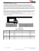
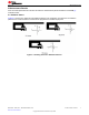
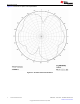


Table Of Contents

1 Description of the antenna Design
It is important to make an exact copy of the antenna dimensions to obtain optimum performance. The
easiest approach to implement the antenna in a PCB CAD tool is to import the antenna layout from a
gerber file or a DXF file. Such files are included in CC2430DB reference design [1]. The gerber file is called
Inverted_F_Antenna.spl and the DXF file is called Inverted_F_Antenna.dxf. If the antenna is implemented on a
PCB that is wider than the antenna, avoid placing components or having a ground plane close to the end points
of the antenna. If the CAD tool being used does not support importing gerber or DXF files, see Figure 1-1 and
Table 1-1.
The antenna impedance is tuned to 50 ohm on the reference board. The impedance will however be affected by
different size and shape of the ground plane, objects in the antenna nearfield such as mechanical assemblies
(housing, batteries, etc.), PCB thickness, PCB material and so on. It is therefore recommended to add a
pi-network close to the antenna feedpoint for impedance matching.
The results presented in this document are based on an antenna implemented on a PCB with a 1-mm thickness
using standard FR-4 material.
Figure 1-1. IFA Dimensions
Table 1-1. IFA Dimensions
H1 5.70 mm W2 0.46 mm
H2 0.74 mm L1 25.58 mm
H3 1.29 mm L2 16.40 mm
H4 2.21 mm L3 2.18 mm
H5 0.66 mm L4 4.80 mm
H6 1.21 mm L5 1.00 mm
H7 0.80 mm L6 1.00 mm
H8 1.80 mm L7 3.20 mm
H9 0.61 mm L8 0.45 mm
W1 1.21 mm
Description of the antenna Design www.ti.com
2 2.4-GHz Inverted F Antenna SWRU120D – APRIL 2007 – REVISED JANUARY 2019
Submit Document Feedback
Copyright © 2021 Texas Instruments Incorporated